AD9956/PCB Analog Devices Inc, AD9956/PCB Datasheet - Page 30
AD9956/PCB
Manufacturer Part Number
AD9956/PCB
Description
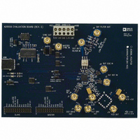
BOARD EVAL FOR AD9956
Manufacturer
Analog Devices Inc
Datasheet
1.AD9956YCPZ.pdf
(32 pages)
Specifications of AD9956/PCB
Module/board Type
Evaluation Board
For Use With/related Products
AD9956
Lead Free Status / RoHS Status
Contains lead / RoHS non-compliant


AD9956
CFR2<28:26> Clock Driver Falling Edge Control
These bits control the slew rate of the CML clock driver output’s
falling edge. When these bits are on, additional current is sent to
the output driver to increase the rising edge slew rate capability.
Table 7 describes how the bits increase the current; the contri-
butions of each bit are cumulative. Note that the additional cur-
rent is on only during the rising edge of the waveform, for ap-
proximately 250 ps, but not on during the entire transition.
Table 7. CML Clock Drive Falling Edge Slew Rate
Control Bits and Associated Surge Current
CFR2<28> = 1
CFR2<30> = 1
CFR2<29> = 1
CFR2<25> PLL_LOCK_DETECT Enable
This bit enables the PLL_LOCK/SYNC_IN pin as a lock detect
output for the PLL.
CFR2<25> = 0 (default).The PLL_LOCK_DETECT signal is
disabled.
CFR2<25> = 1. The PLL_LOCK_DETECT signal is enabled.
CFR2<24> PLL_LOCK_DETECT Mode
This bit toggles the modes of the PLL_LOCK_DETECT func-
tion. The lock detect can either be a status indicator (locked or
unlocked), or it can indicate a lead-lag relationship between the
two phase frequency detector inputs.
CFR2<24> = 0 (default). The lock detect acts as a status indica-
tor (PLL is locked 0 or unlocked 1).
CFR2<24> = 1. The lock detect acts as a lead/lag indicator. A
1 on the PLL_LOCK pin means that the PLLOSC pin lags the
reference. A 0 means that the PLLOSC pin leads the reference.
CFR2<23> RF Divider Power-Down
This bit powers the RF divider down to save power when not in
used.
CFR2<23> = 0 (default). RF divider is on.
CFR2<23> = 1. RF divider is powered down and an alternate
path between the REFCLK inputs and SYSCLK is enabled.
CFR2<22:21> RF Divider Ratio
These two bits control the RF divider ratio (÷R).
CFR2<22:21> = 11 (default). RF Divider R = 8.
CFR2<22:21> = 10. RF Divider R= 4.
CFR2<22:21> = 01. RF Divider R = 2.
5.4 mA
2.7 mA
1.35 mA
Rev. A | Page 30 of 32
CFR2<22:21> = 00. RF Divider R = 1. Note that this is not the
same as bypassing the RF divider.
CFR2<20> Clock Driver Power-Down
This bit powers down the CML clock driver circuit.
CFR2<20> =1 (default). CML clock driver circuit is powered down.
CFR2<20> = 0. CML clock driver is powered up.
CFR2<19:18> Clock Driver Input Select
These bits control the mux on the input for the CML clock driver.
CFR2<19:18> = 00. The CML clock driver is disconnected from
all inputs (and does not toggle).
CFR2<19:18> = 01. The CML clock driver is driven by the
PLLOSC input pin.
CFR2<19:18> = 10 (default). The CML clock driver is driven by
the output of the RF divider.
CFR2<19:18> = 11. The CML clock driver is driven by the input
of the RF divider
CFR2<17> Slew Rate Control Bit
Even without the additional surge current supplied by the rising
edge slew rate control bits and the falling edge slew rate control
bits, the device applies a default 7.6 mA surge current to the
rising edge and a 4.05 mA surge current to the falling edge. This
bit disables all slew rate enhancement surge current, including
the default values.
CFR2<17> = 0 (default). The CML driver applies default surge
current to rising and falling edges.
CFR2<17> = 1. Driver applies no surge current during transi-
tions. The only current is the continuous current.
CFR2<16> RF Divider SYSCLK Mux Bit
This bit toggles the mux to control whether the RF divider out-
put or input is supplying SYSCLK to the device.
CFR2<16> = 0 (default). The RF divider output supplies the
DDS SYSCLK.
CFR2<16> = 1. The RF divider input supplies the DDS SYSCLK
(bypass the divider). Note that regardless of the condition of the
configuration of the clock input, the DDS SYSCLK must not
exceed the maximum rated clock speed.
Related parts for AD9956/PCB
Image
Part Number
Description
Manufacturer
Datasheet
Request
R

Part Number:
Description:
400 Msps 14 Bit DDS EvBd. W/2450MHz VCO
Manufacturer:
Analog Devices Inc
Datasheet:
Part Number:
Description:
400 Msps 14 Bit DDS Eval Bd.
Manufacturer:
Analog Devices Inc
Datasheet:
Part Number:
Description:
BOARD EVAL 14BIT 1.8V 48LFCSP
Manufacturer:
Analog Devices Inc
Datasheet:


Part Number:
Description:
±1.7g Dual-Axis IMEMS Accelerometer Evaluation Board
Manufacturer:
Analog Devices Inc
Datasheet:
Part Number:
Description:
Inertial Sensor Evaluation System
Manufacturer:
Analog Devices Inc
Datasheet:
Part Number:
Description:
Manufacturer:
Analog Devices Inc
Datasheet:
Part Number:
Description:
Manufacturer:
Analog Devices Inc
Datasheet:
Part Number:
Description:
Manufacturer:
Analog Devices Inc
Datasheet:
Part Number:
Description:
Manufacturer:
Analog Devices Inc
Datasheet:
Part Number:
Description:
Manufacturer:
Analog Devices Inc
Datasheet:
Part Number:
Description:
Manufacturer:
Analog Devices Inc
Datasheet:
Part Number:
Description:
Manufacturer:
Analog Devices Inc
Datasheet: