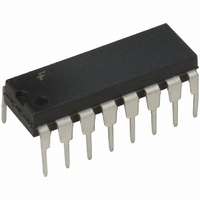
CD4046BCN Fairchild Semiconductor, CD4046BCN Datasheet

CD4046BCN
Specifications of CD4046BCN
4046B
CD4046
Related parts for CD4046BCN
CD4046BCN Summary of contents
Page 1
... Package Number CD4046BCM M16A 16-Lead Small Outline Integrated Circuit (SOIC), JEDEC MS-012, 0.150" Narrow CD4046BCN N16E 16-Lead Plastic Dual-In-Line Package (PDIP), JEDEC MS-001, 0.300" Wide Devices also available in Tape and Reel. Specify by appending the suffix letter “X” to the ordering code. ...
Page 2
Connection Diagram Block Diagram www.fairchildsemi.com Top View FIGURE 1. 2 ...
Page 3
Absolute Maximum Ratings (Note 2) DC Supply Voltage ( Input Voltage ( Storage Temperature Range ( Power Dissipation ( Dual-In-Line Small Outline Lead Temperature ( (Soldering, 10 ...
Page 4
AC Electrical Characteristics Symbol Parameter VCO SECTION I Operating Current DD f Maximum Operating Frequency MAX Linearity Temperature-Frequency Stability No Frequency Offset MIN Frequency Offset, f MIN VCO Input Resistance ...
Page 5
AC Electrical Characteristics Symbol Parameter VCO Offset Voltage IN V DEM Linearity ZENER DIODE V Zener Diode Voltage Z R Zener Dynamic Resistance Z Note 5: AC Parameters are guaranteed by DC correlated testing. Phase Comparator State Diagrams (Continued) Conditions ...
Page 6
Typical Waveforms FIGURE 3. Typical Waveform Employing Phase Comparator I in Locked Condition FIGURE 4. Typical Waveform Employing Phase Comparator II in Locked Condition www.fairchildsemi.com 6 ...
Page 7
Typical Performance Characteristics Note: To obtain approximate total power dissipation of PLL system for no-signal input: Phase Comparator I, P Comparator II, P (Total MIN Typical Center Frequency vs C1 for ...
Page 8
Typical Performance Characteristics Note: To obtain approximate total power dissipation of PLL system for no-signal input: Phase Comparator I, P Comparator II, P (Total MIN www.fairchildsemi.com (Continued) Typical R2/R1 MAX MIN FIGURE ...
Page 9
Typical Performance Characteristics Typical VCO Power Dissipation at f Typical Source Follower Power Dissipation vs R Note: To obtain approximate total power dissipation of PLL system for no-signal input: Phase Comparator I, P Comparator II, P (Total ...
Page 10
Typical Performance Characteristics FIGURE 11. Typical VCO Linearity vs R1 and C1 Note: To obtain approximate total power dissipation of PLL system for no-signal input: Phase Comparator I, P Comparator II, P (Total MIN www.fairchildsemi.com ...
Page 11
Design Information This information is a guide for approximating the value of external components for the CD4046B in a phase-locked- loop system. The selected external components must be within the following ranges: R1 ...
Page 12
Design Information (Continued) Using Phase Comparator I Characteristics VCO Without Offset R2 VCO Component Given Selection Use f with o Figure 5 to determine R1 and C1. References G.S. Moschytz, “Miniaturized RC Filters Using Phase-Locked Loop”, BSTJ, ...
Page 13
Physical Dimensions inches (millimeters) unless otherwise noted 16-Lead Small Outline Integrated Circuit (SOIC), JEDEC MS-012, 0.150" Narrow Package Number M16A 13 www.fairchildsemi.com ...
Page 14
Physical Dimensions inches (millimeters) unless otherwise noted (Continued) 16-Lead Plastic Dual-In-Line Package (PDIP), JEDEC MS-001, 0.300" Wide Fairchild does not assume any responsibility for use of any circuitry described, no circuit patent licenses are implied and Fairchild reserves the right ...


