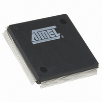
AT91SAM9XE128-QU Atmel, AT91SAM9XE128-QU Datasheet - Page 204

AT91SAM9XE128-QU
Manufacturer Part Number
AT91SAM9XE128-QU
Description
MCU ARM9 128K FLASH 208-PQFP
Manufacturer
Atmel
Series
AT91SAMr
Specifications of AT91SAM9XE128-QU
Core Processor
ARM9
Core Size
16/32-Bit
Speed
180MHz
Connectivity
EBI/EMI, Ethernet, I²C, MMC, SPI, SSC, UART/USART, USB
Peripherals
Brown-out Detect/Reset, POR, PWM, WDT
Number Of I /o
96
Program Memory Size
128KB (128K x 8)
Program Memory Type
FLASH
Ram Size
40K x 8
Voltage - Supply (vcc/vdd)
1.65 V ~ 1.95 V
Data Converters
A/D 4x10b
Oscillator Type
Internal
Operating Temperature
-40°C ~ 85°C
Package / Case
208-MQFP, 208-PQFP
Processor Series
AT91SAMx
Core
ARM926EJ-S
Data Bus Width
32 bit
Data Ram Size
16 KB
Interface Type
2-Wire, EBI, I2S, SPI, USART
Maximum Clock Frequency
180 MHz
Number Of Programmable I/os
96
Number Of Timers
6
Maximum Operating Temperature
+ 85 C
Mounting Style
SMD/SMT
3rd Party Development Tools
JTRACE-ARM-2M, KSK-AT91SAM9XE-PL, MDK-ARM, RL-ARM, ULINK2
Development Tools By Supplier
AT91SAM-ICE, AT91-ISP, AT91SAM9XE-EK
Minimum Operating Temperature
- 40 C
On-chip Adc
10 bit, 4 Channel
For Use With
AT91SAM9XE-EK - KIT EVAL FOR AT91SAM9XEAT91SAM-ICE - EMULATOR FOR AT91 ARM7/ARM9
Lead Free Status / RoHS Status
Lead free / RoHS Compliant
Eeprom Size
-
Lead Free Status / Rohs Status
Lead free / RoHS Compliant
Available stocks
Company
Part Number
Manufacturer
Quantity
Price
- Current page: 204 of 860
- Download datasheet (13Mb)
23.8.1.5
23.8.2
23.8.2.1
204
AT91SAM9XE128/256/512 Preliminary
Read Mode
Null Pulse
Read is Controlled by NRD (READ_MODE = 1):
Figure 23-9. No Setup, No Hold On NRD and NCS Read Signals
Programming null pulse is not permitted. Pulse must be at least set to 1. A null value leads to
unpredictable behavior.
As NCS and NRD waveforms are defined independently of one other, the SMC needs to know
when the read data is available on the data bus. The SMC does not compare NCS and NRD tim-
ings to know which signal rises first. The READ_MODE parameter in the SMC_MODE register
of the corresponding chip select indicates which signal of NRD and NCS controls the read
operation.
Figure 23-10
read data is available t
NRD. In this case, the READ_MODE must be set to 1 (read is controlled by NRD), to indicate
that data is available with the rising edge of NRD. The SMC samples the read data internally on
the rising edge of Master Clock that generates the rising edge of NRD, whatever the pro-
grammed waveform of NCS may be.
NBS0,NBS1,
NBS2,NBS3,
A0, A1
D[31:0]
A[25:2]
MCK
NRD
NCS
shows the waveforms of a read operation of a typical asynchronous RAM. The
PACC
NCS_RD_PULSE
NRD_CYCLE
NRD_PULSE
after the falling edge of NRD, and turns to ‘Z’ after the rising edge of
NCS_RD_PULSE
NRD_PULSE
NRD_CYCLE
NCS_RD_PULSE
NRD_CYCLE
NRD_PULSE
6254C–ATARM–22-Jan-10
Related parts for AT91SAM9XE128-QU
Image
Part Number
Description
Manufacturer
Datasheet
Request
R

Part Number:
Description:
KIT EVAL FOR AT91SAM9XE
Manufacturer:
Atmel
Datasheet:

Part Number:
Description:
MCU ARM9 64K SRAM 144-LFBGA
Manufacturer:
Atmel
Datasheet:

Part Number:
Description:
IC ARM7 MCU FLASH 256K 100LQFP
Manufacturer:
Atmel
Datasheet:

Part Number:
Description:
IC ARM9 MPU 217-LFBGA
Manufacturer:
Atmel
Datasheet:

Part Number:
Description:
MCU ARM9 ULTRA LOW PWR 217-LFBGA
Manufacturer:
Atmel
Datasheet:

Part Number:
Description:
MCU ARM9 324-TFBGA
Manufacturer:
Atmel
Datasheet:

Part Number:
Description:
IC MCU ARM9 SAMPLING 217CBGA
Manufacturer:
Atmel
Datasheet:

Part Number:
Description:
IC ARM9 MCU 217-LFBGA
Manufacturer:
Atmel
Datasheet:

Part Number:
Description:
IC ARM9 MCU 208-PQFP
Manufacturer:
Atmel
Datasheet:

Part Number:
Description:
MCU ARM 512K HS FLASH 100-LQFP
Manufacturer:
Atmel
Datasheet:

Part Number:
Description:
MCU ARM 512K HS FLASH 100-TFBGA
Manufacturer:
Atmel
Datasheet:

Part Number:
Description:
IC ARM9 MCU 200 MHZ 324-TFBGA
Manufacturer:
Atmel
Datasheet:

Part Number:
Description:
IC ARM MCU 16BIT 128K 256BGA
Manufacturer:
Atmel
Datasheet:

Part Number:
Description:
IC ARM7 MCU 32BIT 128K 64LQFP
Manufacturer:
Atmel
Datasheet:

Part Number:
Description:
IC ARM7 MCU FLASH 256K 128-LQFP
Manufacturer:
Atmel
Datasheet:


