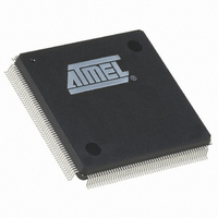
AT91SAM9XE128-QU Atmel, AT91SAM9XE128-QU Datasheet - Page 716

AT91SAM9XE128-QU
Manufacturer Part Number
AT91SAM9XE128-QU
Description
MCU ARM9 128K FLASH 208-PQFP
Manufacturer
Atmel
Series
AT91SAMr
Specifications of AT91SAM9XE128-QU
Core Processor
ARM9
Core Size
16/32-Bit
Speed
180MHz
Connectivity
EBI/EMI, Ethernet, I²C, MMC, SPI, SSC, UART/USART, USB
Peripherals
Brown-out Detect/Reset, POR, PWM, WDT
Number Of I /o
96
Program Memory Size
128KB (128K x 8)
Program Memory Type
FLASH
Ram Size
40K x 8
Voltage - Supply (vcc/vdd)
1.65 V ~ 1.95 V
Data Converters
A/D 4x10b
Oscillator Type
Internal
Operating Temperature
-40°C ~ 85°C
Package / Case
208-MQFP, 208-PQFP
Processor Series
AT91SAMx
Core
ARM926EJ-S
Data Bus Width
32 bit
Data Ram Size
16 KB
Interface Type
2-Wire, EBI, I2S, SPI, USART
Maximum Clock Frequency
180 MHz
Number Of Programmable I/os
96
Number Of Timers
6
Maximum Operating Temperature
+ 85 C
Mounting Style
SMD/SMT
3rd Party Development Tools
JTRACE-ARM-2M, KSK-AT91SAM9XE-PL, MDK-ARM, RL-ARM, ULINK2
Development Tools By Supplier
AT91SAM-ICE, AT91-ISP, AT91SAM9XE-EK
Minimum Operating Temperature
- 40 C
On-chip Adc
10 bit, 4 Channel
For Use With
AT91SAM9XE-EK - KIT EVAL FOR AT91SAM9XEAT91SAM-ICE - EMULATOR FOR AT91 ARM7/ARM9
Lead Free Status / RoHS Status
Lead free / RoHS Compliant
Eeprom Size
-
Lead Free Status / Rohs Status
Lead free / RoHS Compliant
Available stocks
Company
Part Number
Manufacturer
Quantity
Price
- Current page: 716 of 860
- Download datasheet (13Mb)
Figure 39-8. Data IN Transfer for Ping-pong Endpoint
716
TXPKTRDY Flag
(UDP_MCSRx)
FIFO (DPR)
Bank 0
FIFO (DPR)
USB Bus
Packets
TXCOMP Flag
(UDP_CSRx)
Bank 1
AT91SAM9XE128/256/512 Preliminary
Written by
Microcontroller
Microcontroller
Load Data IN Bank 0
Set by Firmware,
Data Payload Written in FIFO Bank 0
When using a ping-pong endpoint, the following procedures are required to perform Data IN
transactions:
Warning: There is software critical path due to the fact that once the second bank is filled, the
driver has to wait for TX_COMP to set TX_PKTRDY. If the delay between receiving TX_COMP
is set and TX_PKTRDY is set too long, some Data IN packets may be NACKed, reducing the
bandwidth.
Warning: TX_COMP must be cleared after TX_PKTRDY has been set.
1. The microcontroller checks if it is possible to write in the FIFO by polling TXPKTRDY to
2. The microcontroller writes the first data payload to be sent in the FIFO (Bank 0), writing
3. The microcontroller notifies the USB peripheral it has finished writing in Bank 0 of the
4. Without waiting for TXPKTRDY to be cleared, the microcontroller writes the second
5. The microcontroller is notified that the first Bank has been released by the USB device
6. Once the microcontroller has received TXCOMP for the first Bank, it notifies the USB
7. At this step, Bank 0 is available and the microcontroller can prepare a third data pay-
Data IN
PID
be cleared in the endpoint’s UDP_CSRx register.
zero or more byte values in the endpoint’s UDP_FDRx register.
FIFO by setting the TXPKTRDY in the endpoint’s UDP_CSRx register.
data payload to be sent in the FIFO (Bank 1), writing zero or more byte values in the
endpoint’s UDP_FDRx register.
when TXCOMP in the endpoint’s UDP_CSRx register is set. An interrupt is pending
while TXCOMP is being set.
device that it has prepared the second Bank to be sent, raising TXPKTRDY in the end-
point’s UDP_CSRx register.
load to be sent
Microcontroller Load Data IN Bank 1
USB Device Send Bank 0
Written by
Microcontroller
Read by USB Device
Data IN
Cleared by USB Device,
Data Payload Fully Transmitted
.
Set by USB
Device
ACK
PID
Interrupt Cleared by Firmware
Data IN
PID
Microcontroller Load Data IN Bank 0
USB Device Send Bank 1
Interrupt Pending
Written by
Microcontroller
Set by Firmware,
Data Payload Written in FIFO Bank 1
Read by USB Device
Data IN
Set by USB Device
6254C–ATARM–22-Jan-10
ACK
PID
Related parts for AT91SAM9XE128-QU
Image
Part Number
Description
Manufacturer
Datasheet
Request
R

Part Number:
Description:
KIT EVAL FOR AT91SAM9XE
Manufacturer:
Atmel
Datasheet:

Part Number:
Description:
MCU ARM9 64K SRAM 144-LFBGA
Manufacturer:
Atmel
Datasheet:

Part Number:
Description:
IC ARM7 MCU FLASH 256K 100LQFP
Manufacturer:
Atmel
Datasheet:

Part Number:
Description:
IC ARM9 MPU 217-LFBGA
Manufacturer:
Atmel
Datasheet:

Part Number:
Description:
MCU ARM9 ULTRA LOW PWR 217-LFBGA
Manufacturer:
Atmel
Datasheet:

Part Number:
Description:
MCU ARM9 324-TFBGA
Manufacturer:
Atmel
Datasheet:

Part Number:
Description:
IC MCU ARM9 SAMPLING 217CBGA
Manufacturer:
Atmel
Datasheet:

Part Number:
Description:
IC ARM9 MCU 217-LFBGA
Manufacturer:
Atmel
Datasheet:

Part Number:
Description:
IC ARM9 MCU 208-PQFP
Manufacturer:
Atmel
Datasheet:

Part Number:
Description:
MCU ARM 512K HS FLASH 100-LQFP
Manufacturer:
Atmel
Datasheet:

Part Number:
Description:
MCU ARM 512K HS FLASH 100-TFBGA
Manufacturer:
Atmel
Datasheet:

Part Number:
Description:
IC ARM9 MCU 200 MHZ 324-TFBGA
Manufacturer:
Atmel
Datasheet:

Part Number:
Description:
IC ARM MCU 16BIT 128K 256BGA
Manufacturer:
Atmel
Datasheet:

Part Number:
Description:
IC ARM7 MCU 32BIT 128K 64LQFP
Manufacturer:
Atmel
Datasheet:

Part Number:
Description:
IC ARM7 MCU FLASH 256K 128-LQFP
Manufacturer:
Atmel
Datasheet:


