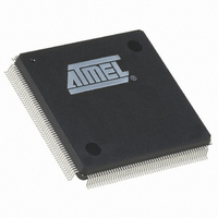
AT91SAM9XE128-QU Atmel, AT91SAM9XE128-QU Datasheet - Page 209

AT91SAM9XE128-QU
Manufacturer Part Number
AT91SAM9XE128-QU
Description
MCU ARM9 128K FLASH 208-PQFP
Manufacturer
Atmel
Series
AT91SAMr
Specifications of AT91SAM9XE128-QU
Core Processor
ARM9
Core Size
16/32-Bit
Speed
180MHz
Connectivity
EBI/EMI, Ethernet, I²C, MMC, SPI, SSC, UART/USART, USB
Peripherals
Brown-out Detect/Reset, POR, PWM, WDT
Number Of I /o
96
Program Memory Size
128KB (128K x 8)
Program Memory Type
FLASH
Ram Size
40K x 8
Voltage - Supply (vcc/vdd)
1.65 V ~ 1.95 V
Data Converters
A/D 4x10b
Oscillator Type
Internal
Operating Temperature
-40°C ~ 85°C
Package / Case
208-MQFP, 208-PQFP
Processor Series
AT91SAMx
Core
ARM926EJ-S
Data Bus Width
32 bit
Data Ram Size
16 KB
Interface Type
2-Wire, EBI, I2S, SPI, USART
Maximum Clock Frequency
180 MHz
Number Of Programmable I/os
96
Number Of Timers
6
Maximum Operating Temperature
+ 85 C
Mounting Style
SMD/SMT
3rd Party Development Tools
JTRACE-ARM-2M, KSK-AT91SAM9XE-PL, MDK-ARM, RL-ARM, ULINK2
Development Tools By Supplier
AT91SAM-ICE, AT91-ISP, AT91SAM9XE-EK
Minimum Operating Temperature
- 40 C
On-chip Adc
10 bit, 4 Channel
For Use With
AT91SAM9XE-EK - KIT EVAL FOR AT91SAM9XEAT91SAM-ICE - EMULATOR FOR AT91 ARM7/ARM9
Lead Free Status / RoHS Status
Lead free / RoHS Compliant
Eeprom Size
-
Lead Free Status / Rohs Status
Lead free / RoHS Compliant
Available stocks
Company
Part Number
Manufacturer
Quantity
Price
- Current page: 209 of 860
- Download datasheet (13Mb)
23.8.5
Table 23-4.
6254C–ATARM–22-Jan-10
Coded Value
setup [5:0]
pulse [6:0]
cycle [8:0]
Coding Timing Parameters
Coding and Range of Timing Parameters
Number of Bits
Figure 23-15. WRITE_MODE = 0. The write operation is controlled by NCS
All timing parameters are defined for one chip select and are grouped together in one
SMC_REGISTER according to their type.
The SMC_SETUP register groups the definition of all setup parameters:
• NRD_SETUP, NCS_RD_SETUP, NWE_SETUP, NCS_WR_SETUP
The SMC_PULSE register groups the definition of all pulse parameters:
• NRD_PULSE, NCS_RD_PULSE, NWE_PULSE, NCS_WR_PULSE
The SMC_CYCLE register groups the definition of all cycle parameters:
• NRD_CYCLE, NWE_CYCLE
Table 23-4
6
7
9
NWR0, NWR1,
NWR2, NWR3
NBS0, NBS1,
NBS2, NBS3,
A0, A1
D[31:0]
A
shows how the timing parameters are coded and their permitted range.
NWE,
[25:2]
MCK
NCS
256 x cycle[8:7] + cycle[6:0]
128 x setup[5] + setup[4:0]
256 x pulse[6] + pulse[5:0]
Effective Value
AT91SAM9XE128/256/512 Preliminary
Coded Value
0 ≤ ≤ 127
0 ≤ ≤ 31
0 ≤ ≤ 63
Permitted Range
Effective Value
0 ≤ ≤ 256+127
0 ≤ ≤ 512+127
0 ≤ ≤ 768+127
0 ≤ ≤ 128+31
0 ≤ ≤ 256+63
209
Related parts for AT91SAM9XE128-QU
Image
Part Number
Description
Manufacturer
Datasheet
Request
R

Part Number:
Description:
KIT EVAL FOR AT91SAM9XE
Manufacturer:
Atmel
Datasheet:

Part Number:
Description:
MCU ARM9 64K SRAM 144-LFBGA
Manufacturer:
Atmel
Datasheet:

Part Number:
Description:
IC ARM7 MCU FLASH 256K 100LQFP
Manufacturer:
Atmel
Datasheet:

Part Number:
Description:
IC ARM9 MPU 217-LFBGA
Manufacturer:
Atmel
Datasheet:

Part Number:
Description:
MCU ARM9 ULTRA LOW PWR 217-LFBGA
Manufacturer:
Atmel
Datasheet:

Part Number:
Description:
MCU ARM9 324-TFBGA
Manufacturer:
Atmel
Datasheet:

Part Number:
Description:
IC MCU ARM9 SAMPLING 217CBGA
Manufacturer:
Atmel
Datasheet:

Part Number:
Description:
IC ARM9 MCU 217-LFBGA
Manufacturer:
Atmel
Datasheet:

Part Number:
Description:
IC ARM9 MCU 208-PQFP
Manufacturer:
Atmel
Datasheet:

Part Number:
Description:
MCU ARM 512K HS FLASH 100-LQFP
Manufacturer:
Atmel
Datasheet:

Part Number:
Description:
MCU ARM 512K HS FLASH 100-TFBGA
Manufacturer:
Atmel
Datasheet:

Part Number:
Description:
IC ARM9 MCU 200 MHZ 324-TFBGA
Manufacturer:
Atmel
Datasheet:

Part Number:
Description:
IC ARM MCU 16BIT 128K 256BGA
Manufacturer:
Atmel
Datasheet:

Part Number:
Description:
IC ARM7 MCU 32BIT 128K 64LQFP
Manufacturer:
Atmel
Datasheet:

Part Number:
Description:
IC ARM7 MCU FLASH 256K 128-LQFP
Manufacturer:
Atmel
Datasheet:


