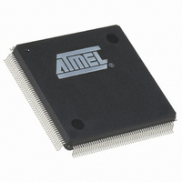
AT91SAM9XE128-QU Atmel, AT91SAM9XE128-QU Datasheet - Page 671

AT91SAM9XE128-QU
Manufacturer Part Number
AT91SAM9XE128-QU
Description
MCU ARM9 128K FLASH 208-PQFP
Manufacturer
Atmel
Series
AT91SAMr
Specifications of AT91SAM9XE128-QU
Core Processor
ARM9
Core Size
16/32-Bit
Speed
180MHz
Connectivity
EBI/EMI, Ethernet, I²C, MMC, SPI, SSC, UART/USART, USB
Peripherals
Brown-out Detect/Reset, POR, PWM, WDT
Number Of I /o
96
Program Memory Size
128KB (128K x 8)
Program Memory Type
FLASH
Ram Size
40K x 8
Voltage - Supply (vcc/vdd)
1.65 V ~ 1.95 V
Data Converters
A/D 4x10b
Oscillator Type
Internal
Operating Temperature
-40°C ~ 85°C
Package / Case
208-MQFP, 208-PQFP
Processor Series
AT91SAMx
Core
ARM926EJ-S
Data Bus Width
32 bit
Data Ram Size
16 KB
Interface Type
2-Wire, EBI, I2S, SPI, USART
Maximum Clock Frequency
180 MHz
Number Of Programmable I/os
96
Number Of Timers
6
Maximum Operating Temperature
+ 85 C
Mounting Style
SMD/SMT
3rd Party Development Tools
JTRACE-ARM-2M, KSK-AT91SAM9XE-PL, MDK-ARM, RL-ARM, ULINK2
Development Tools By Supplier
AT91SAM-ICE, AT91-ISP, AT91SAM9XE-EK
Minimum Operating Temperature
- 40 C
On-chip Adc
10 bit, 4 Channel
For Use With
AT91SAM9XE-EK - KIT EVAL FOR AT91SAM9XEAT91SAM-ICE - EMULATOR FOR AT91 ARM7/ARM9
Lead Free Status / RoHS Status
Lead free / RoHS Compliant
Eeprom Size
-
Lead Free Status / Rohs Status
Lead free / RoHS Compliant
Available stocks
Company
Part Number
Manufacturer
Quantity
Price
- Current page: 671 of 860
- Download datasheet (13Mb)
38.4
38.4.1
38.4.1.1
38.4.1.2
Figure 38-2. Receive Buffer List
6254C–ATARM–22-Jan-10
Programming Interface
Initialization
Configuration
Receive Buffer List
Receive Buffer Queue Pointer
(MAC Register)
Initialization of the EMAC configuration (e.g., loop-back mode, frequency ratios) must be done
while the transmit and receive circuits are disabled. See the description of the network control
register and network configuration register earlier in this document.
To change loop-back mode, the following sequence of operations must be followed:
Note:
Receive data is written to areas of data (i.e., buffers) in system memory. These buffers are listed
in another data structure that also resides in main memory. This data structure (receive buffer
queue) is a sequence of descriptor entries as defined in
page
To create the list of buffers:
1. Write to network control register to disable transmit and receive circuits.
2. Write to network control register to change loop-back mode.
3. Write to network control register to re-enable transmit or receive circuits.
1. Allocate a number (n) of buffers of 128 bytes in system memory.
2. Allocate an area 2n words for the receive buffer descriptor entry in system memory and
3. If less than 1024 buffers are defined, the last descriptor must be marked with the wrap
4. Write address of receive buffer descriptor entry to EMAC register receive_buffer
5. The receive circuits can then be enabled by writing to the address recognition registers
661. It points to this data structure.
create n entries in this list. Mark all entries in this list as owned by EMAC, i.e., bit 0 of
word 0 set to 0.
bit (bit 1 in word 0 set to 1).
queue pointer.
and then to the network control register.
These writes to network control register cannot be combined in any way.
AT91SAM9XE128/256/512 Preliminary
Receive Buffer Descriptor List
(In memory)
“Receive Buffer Descriptor Entry” on
Receive Buffer 1
Receive Buffer 0
Receive Buffer N
(In memory)
671
Related parts for AT91SAM9XE128-QU
Image
Part Number
Description
Manufacturer
Datasheet
Request
R

Part Number:
Description:
KIT EVAL FOR AT91SAM9XE
Manufacturer:
Atmel
Datasheet:

Part Number:
Description:
MCU ARM9 64K SRAM 144-LFBGA
Manufacturer:
Atmel
Datasheet:

Part Number:
Description:
IC ARM7 MCU FLASH 256K 100LQFP
Manufacturer:
Atmel
Datasheet:

Part Number:
Description:
IC ARM9 MPU 217-LFBGA
Manufacturer:
Atmel
Datasheet:

Part Number:
Description:
MCU ARM9 ULTRA LOW PWR 217-LFBGA
Manufacturer:
Atmel
Datasheet:

Part Number:
Description:
MCU ARM9 324-TFBGA
Manufacturer:
Atmel
Datasheet:

Part Number:
Description:
IC MCU ARM9 SAMPLING 217CBGA
Manufacturer:
Atmel
Datasheet:

Part Number:
Description:
IC ARM9 MCU 217-LFBGA
Manufacturer:
Atmel
Datasheet:

Part Number:
Description:
IC ARM9 MCU 208-PQFP
Manufacturer:
Atmel
Datasheet:

Part Number:
Description:
MCU ARM 512K HS FLASH 100-LQFP
Manufacturer:
Atmel
Datasheet:

Part Number:
Description:
MCU ARM 512K HS FLASH 100-TFBGA
Manufacturer:
Atmel
Datasheet:

Part Number:
Description:
IC ARM9 MCU 200 MHZ 324-TFBGA
Manufacturer:
Atmel
Datasheet:

Part Number:
Description:
IC ARM MCU 16BIT 128K 256BGA
Manufacturer:
Atmel
Datasheet:

Part Number:
Description:
IC ARM7 MCU 32BIT 128K 64LQFP
Manufacturer:
Atmel
Datasheet:

Part Number:
Description:
IC ARM7 MCU FLASH 256K 128-LQFP
Manufacturer:
Atmel
Datasheet:


