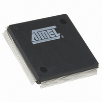
AT91SAM9XE128-QU Atmel, AT91SAM9XE128-QU Datasheet - Page 838

AT91SAM9XE128-QU
Manufacturer Part Number
AT91SAM9XE128-QU
Description
MCU ARM9 128K FLASH 208-PQFP
Manufacturer
Atmel
Series
AT91SAMr
Specifications of AT91SAM9XE128-QU
Core Processor
ARM9
Core Size
16/32-Bit
Speed
180MHz
Connectivity
EBI/EMI, Ethernet, I²C, MMC, SPI, SSC, UART/USART, USB
Peripherals
Brown-out Detect/Reset, POR, PWM, WDT
Number Of I /o
96
Program Memory Size
128KB (128K x 8)
Program Memory Type
FLASH
Ram Size
40K x 8
Voltage - Supply (vcc/vdd)
1.65 V ~ 1.95 V
Data Converters
A/D 4x10b
Oscillator Type
Internal
Operating Temperature
-40°C ~ 85°C
Package / Case
208-MQFP, 208-PQFP
Processor Series
AT91SAMx
Core
ARM926EJ-S
Data Bus Width
32 bit
Data Ram Size
16 KB
Interface Type
2-Wire, EBI, I2S, SPI, USART
Maximum Clock Frequency
180 MHz
Number Of Programmable I/os
96
Number Of Timers
6
Maximum Operating Temperature
+ 85 C
Mounting Style
SMD/SMT
3rd Party Development Tools
JTRACE-ARM-2M, KSK-AT91SAM9XE-PL, MDK-ARM, RL-ARM, ULINK2
Development Tools By Supplier
AT91SAM-ICE, AT91-ISP, AT91SAM9XE-EK
Minimum Operating Temperature
- 40 C
On-chip Adc
10 bit, 4 Channel
For Use With
AT91SAM9XE-EK - KIT EVAL FOR AT91SAM9XEAT91SAM-ICE - EMULATOR FOR AT91 ARM7/ARM9
Lead Free Status / RoHS Status
Lead free / RoHS Compliant
Eeprom Size
-
Lead Free Status / Rohs Status
Lead free / RoHS Compliant
Available stocks
Company
Part Number
Manufacturer
Quantity
Price
- Current page: 838 of 860
- Download datasheet (13Mb)
46.2
46.2.1
46.2.1.1
46.2.2
46.2.2.1
46.2.3
46.2.3.1
46.2.3.2
46.2.3.3
46.2.3.4
838
AT91SAM9XE128/256/512 Errata - Revision A parts
AT91SAM9XE128/256/512 Preliminary
Analog-to-Digital Converter (ADC)
Error Corrected Code Controller (ECC)
MultiMedia Card Interface (MCI)
ADC: Sleep Mode
ECC: Computation with a 1 clock cycle long NRD/NWE pulse
MCI: Busy signal of R1b responses is not taken in account
MCI: SDIO Interrupt does not work with slots other than A
MCI: Data Write Operation and number of bytes
MCI: Flag Reset is not correct in half duplex mode
Refer to
If Sleep mode is activated while there is no activity (no conversion is being performed), it will
take effect only after a conversion occurs.
To activate sleep mode as soon as possible, it is recommended to write successively, ADC
Mode Register (SLEEP) then ADC Control Register (START bit field), in order to start an analog-
to-digital conversion and then put ADC into sleep mode at the end of this conversion.
If the SMC is programmed with NRD/NWE pulse length equal to 1 clock cycle, HECC can't com-
pute the parity.
It is recommended to program SMC with a value higher than 1.
The busy status of the card during the response (R1b) is ignored for the commands CMD7,
CMD28, CMD29, CMD38, CMD42, CMD56. Additionally, for commands CMD42 and CMD56 a
conflict can occur on data line0 if the MCI sends data to the card while the card is still busy. The
behavior is correct for CMD12 command (STOP_TRANSFER).
None
If there is 1-bit data bus width on slots other than slot A, the SDIO interrupt can not be captured.
The sample is made on the wrong data line.
Problem Fix/Workaround
None
The Data Write operation with a number of bytes less than 12 is impossible.
The PDC counters must always be equal to 12 bytes for data transfers lower than 12 bytes. The
BLKLEN or BCNT field are used to specify the real count number.
In half duplex mode, the reset of the flags ENDRX, RXBUFF, ENDTX and TXBUFE can be
incorrect. These flags are reset correctly after a PDC channel enable.
Problem Fix/Workaround
Problem/Fix Workaround
Problem Fix/Workaround
Problem Fix/Workaround
Problem Fix/Workaround
Section 46.1 “Marking” on page
837.
6254C–ATARM–22-Jan-10
Related parts for AT91SAM9XE128-QU
Image
Part Number
Description
Manufacturer
Datasheet
Request
R

Part Number:
Description:
KIT EVAL FOR AT91SAM9XE
Manufacturer:
Atmel
Datasheet:

Part Number:
Description:
MCU ARM9 64K SRAM 144-LFBGA
Manufacturer:
Atmel
Datasheet:

Part Number:
Description:
IC ARM7 MCU FLASH 256K 100LQFP
Manufacturer:
Atmel
Datasheet:

Part Number:
Description:
IC ARM9 MPU 217-LFBGA
Manufacturer:
Atmel
Datasheet:

Part Number:
Description:
MCU ARM9 ULTRA LOW PWR 217-LFBGA
Manufacturer:
Atmel
Datasheet:

Part Number:
Description:
MCU ARM9 324-TFBGA
Manufacturer:
Atmel
Datasheet:

Part Number:
Description:
IC MCU ARM9 SAMPLING 217CBGA
Manufacturer:
Atmel
Datasheet:

Part Number:
Description:
IC ARM9 MCU 217-LFBGA
Manufacturer:
Atmel
Datasheet:

Part Number:
Description:
IC ARM9 MCU 208-PQFP
Manufacturer:
Atmel
Datasheet:

Part Number:
Description:
MCU ARM 512K HS FLASH 100-LQFP
Manufacturer:
Atmel
Datasheet:

Part Number:
Description:
MCU ARM 512K HS FLASH 100-TFBGA
Manufacturer:
Atmel
Datasheet:

Part Number:
Description:
IC ARM9 MCU 200 MHZ 324-TFBGA
Manufacturer:
Atmel
Datasheet:

Part Number:
Description:
IC ARM MCU 16BIT 128K 256BGA
Manufacturer:
Atmel
Datasheet:

Part Number:
Description:
IC ARM7 MCU 32BIT 128K 64LQFP
Manufacturer:
Atmel
Datasheet:

Part Number:
Description:
IC ARM7 MCU FLASH 256K 128-LQFP
Manufacturer:
Atmel
Datasheet:


