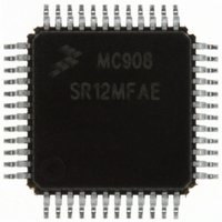
MC908SR12MFAE Freescale Semiconductor, MC908SR12MFAE Datasheet - Page 179

MC908SR12MFAE
Manufacturer Part Number
MC908SR12MFAE
Description
IC MCU 12K FLASH 8MHZ 48-LQFP
Manufacturer
Freescale Semiconductor
Series
HC08r
Datasheet
1.MC908SR12MFAE.pdf
(404 pages)
Specifications of MC908SR12MFAE
Core Processor
HC08
Core Size
8-Bit
Speed
8MHz
Connectivity
I²C, SCI
Peripherals
LVD, POR, PWM, Temp Sensor
Number Of I /o
31
Program Memory Size
12KB (12K x 8)
Program Memory Type
FLASH
Ram Size
512 x 8
Voltage - Supply (vcc/vdd)
4.5 V ~ 5.5 V
Data Converters
A/D 14x10b
Oscillator Type
Internal
Operating Temperature
-40°C ~ 125°C
Package / Case
48-LQFP
Lead Free Status / RoHS Status
Lead free / RoHS Compliant
Eeprom Size
-
Available stocks
Company
Part Number
Manufacturer
Quantity
Price
Company:
Part Number:
MC908SR12MFAE
Manufacturer:
Freescale Semiconductor
Quantity:
10 000
Company:
Part Number:
MC908SR12MFAER
Manufacturer:
Freescale Semiconductor
Quantity:
10 000
- Current page: 179 of 404
- Download datasheet (2Mb)
MC68HC908SR12•MC68HC08SR12 — Rev. 5.0
Freescale Semiconductor
NOTE:
Upon power-on reset, if the received bytes of the security code do not
match the data at locations $FFF6–$FFFD, the host fails to bypass the
security feature. The MCU remains in monitor mode, but reading a
FLASH location returns an invalid value and trying to execute code from
FLASH causes an illegal address reset. After receiving the eight security
bytes from the host, the MCU transmits a break character, signifying that
it is ready to receive a command.
The MCU does not transmit a break character until after the host sends
the eight security bits.
To determine whether the security code entered is correct, check to see
if bit 6 of RAM address $40 is set. If it is, then the correct security code
has been entered and FLASH can be accessed.
If the security sequence fails, the device should be reset by a power-on
reset and brought up in monitor mode to attempt another entry. After
failing the security sequence, the FLASH module can also be mass
erased by executing an erase routine that was downloaded into internal
RAM. The mass erase operation clears the security code locations so
that all eight security bytes become $FF (blank).
PTA0
RST
NOTES:
V
DD
1 = Echo delay, 2 bit times.
2 = Data return delay, 2 bit times.
4 = Wait 1 bit time before sending next byte.
FROM HOST
Figure 10-8. Monitor Mode Entry Timing
FROM MCU
Monitor ROM (MON)
4096 + 32 ICLK CYCLES
1
256 BUS CYCLES (MINIMUM)
4
1
1
Monitor ROM (MON)
2
4
Data Sheet
Security
1
179
Related parts for MC908SR12MFAE
Image
Part Number
Description
Manufacturer
Datasheet
Request
R
Part Number:
Description:
Manufacturer:
Freescale Semiconductor, Inc
Datasheet:
Part Number:
Description:
Manufacturer:
Freescale Semiconductor, Inc
Datasheet:
Part Number:
Description:
Manufacturer:
Freescale Semiconductor, Inc
Datasheet:
Part Number:
Description:
Manufacturer:
Freescale Semiconductor, Inc
Datasheet:
Part Number:
Description:
Manufacturer:
Freescale Semiconductor, Inc
Datasheet:
Part Number:
Description:
Manufacturer:
Freescale Semiconductor, Inc
Datasheet:
Part Number:
Description:
Manufacturer:
Freescale Semiconductor, Inc
Datasheet:
Part Number:
Description:
Manufacturer:
Freescale Semiconductor, Inc
Datasheet:
Part Number:
Description:
Manufacturer:
Freescale Semiconductor, Inc
Datasheet:
Part Number:
Description:
Manufacturer:
Freescale Semiconductor, Inc
Datasheet:
Part Number:
Description:
Manufacturer:
Freescale Semiconductor, Inc
Datasheet:
Part Number:
Description:
Manufacturer:
Freescale Semiconductor, Inc
Datasheet:
Part Number:
Description:
Manufacturer:
Freescale Semiconductor, Inc
Datasheet:
Part Number:
Description:
Manufacturer:
Freescale Semiconductor, Inc
Datasheet:
Part Number:
Description:
Manufacturer:
Freescale Semiconductor, Inc
Datasheet:


