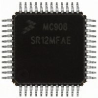
MC908SR12MFAE Freescale Semiconductor, MC908SR12MFAE Datasheet - Page 329

MC908SR12MFAE
Manufacturer Part Number
MC908SR12MFAE
Description
IC MCU 12K FLASH 8MHZ 48-LQFP
Manufacturer
Freescale Semiconductor
Series
HC08r
Datasheet
1.MC908SR12MFAE.pdf
(404 pages)
Specifications of MC908SR12MFAE
Core Processor
HC08
Core Size
8-Bit
Speed
8MHz
Connectivity
I²C, SCI
Peripherals
LVD, POR, PWM, Temp Sensor
Number Of I /o
31
Program Memory Size
12KB (12K x 8)
Program Memory Type
FLASH
Ram Size
512 x 8
Voltage - Supply (vcc/vdd)
4.5 V ~ 5.5 V
Data Converters
A/D 14x10b
Oscillator Type
Internal
Operating Temperature
-40°C ~ 125°C
Package / Case
48-LQFP
Lead Free Status / RoHS Status
Lead free / RoHS Compliant
Eeprom Size
-
Available stocks
Company
Part Number
Manufacturer
Quantity
Price
Company:
Part Number:
MC908SR12MFAE
Manufacturer:
Freescale Semiconductor
Quantity:
10 000
Company:
Part Number:
MC908SR12MFAER
Manufacturer:
Freescale Semiconductor
Quantity:
10 000
- Current page: 329 of 404
- Download datasheet (2Mb)
18.5.2 Data Direction Register C (DDRC)
MC68HC908SR12•MC68HC08SR12 — Rev. 5.0
Freescale Semiconductor
NOTE:
NOTE:
Address:
Data direction register C determines whether each port C pin is an input
or an output. Writing a logic 1 to a DDRC bit enables the output buffer for
the corresponding port C pin; a logic 0 disables the output buffer.
DDRC[7:0] — Data Direction Register C Bits
Avoid glitches on port C pins by writing to the port C data register before
changing data direction register C bits from 0 to 1.
the port C I/O logic.
For those devices packaged in a 42-pin shrink dual in-line package,
PTC6 and PTC7 are not connected. DDRC6 and DDRC7 should be set
to a 1 to configure PTC6 and PTC7 as outputs.
Reset:
Read:
Write:
These read/write bits control port C data direction. Reset clears
DDRC[7:0], configuring all port C pins as inputs.
1 = Corresponding port C pin configured as output
0 = Corresponding port C pin configured as input
DDRC7
READ DDRC ($0006)
WRITE DDRC ($0006)
WRITE PTC ($0002)
READ PTC ($0002)
$0006
Bit 7
Figure 18-10. Data Direction Register B (DDRB)
0
Input/Output (I/O) Ports
DDRC6
6
0
Figure 18-11. Port C I/O Circuit
RESET
DDRC5
5
0
DDRC4
DDRCx
PTCx
4
0
DDRC3
3
0
DDRC2
Figure 18-11
2
0
Input/Output (I/O) Ports
DDRC1
1
0
Data Sheet
shows
DDRC0
Bit 0
Port C
0
PTCx
329
Related parts for MC908SR12MFAE
Image
Part Number
Description
Manufacturer
Datasheet
Request
R
Part Number:
Description:
Manufacturer:
Freescale Semiconductor, Inc
Datasheet:
Part Number:
Description:
Manufacturer:
Freescale Semiconductor, Inc
Datasheet:
Part Number:
Description:
Manufacturer:
Freescale Semiconductor, Inc
Datasheet:
Part Number:
Description:
Manufacturer:
Freescale Semiconductor, Inc
Datasheet:
Part Number:
Description:
Manufacturer:
Freescale Semiconductor, Inc
Datasheet:
Part Number:
Description:
Manufacturer:
Freescale Semiconductor, Inc
Datasheet:
Part Number:
Description:
Manufacturer:
Freescale Semiconductor, Inc
Datasheet:
Part Number:
Description:
Manufacturer:
Freescale Semiconductor, Inc
Datasheet:
Part Number:
Description:
Manufacturer:
Freescale Semiconductor, Inc
Datasheet:
Part Number:
Description:
Manufacturer:
Freescale Semiconductor, Inc
Datasheet:
Part Number:
Description:
Manufacturer:
Freescale Semiconductor, Inc
Datasheet:
Part Number:
Description:
Manufacturer:
Freescale Semiconductor, Inc
Datasheet:
Part Number:
Description:
Manufacturer:
Freescale Semiconductor, Inc
Datasheet:
Part Number:
Description:
Manufacturer:
Freescale Semiconductor, Inc
Datasheet:
Part Number:
Description:
Manufacturer:
Freescale Semiconductor, Inc
Datasheet:


