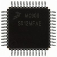
MC908SR12MFAE Freescale Semiconductor, MC908SR12MFAE Datasheet - Page 272

MC908SR12MFAE
Manufacturer Part Number
MC908SR12MFAE
Description
IC MCU 12K FLASH 8MHZ 48-LQFP
Manufacturer
Freescale Semiconductor
Series
HC08r
Datasheet
1.MC908SR12MFAE.pdf
(404 pages)
Specifications of MC908SR12MFAE
Core Processor
HC08
Core Size
8-Bit
Speed
8MHz
Connectivity
I²C, SCI
Peripherals
LVD, POR, PWM, Temp Sensor
Number Of I /o
31
Program Memory Size
12KB (12K x 8)
Program Memory Type
FLASH
Ram Size
512 x 8
Voltage - Supply (vcc/vdd)
4.5 V ~ 5.5 V
Data Converters
A/D 14x10b
Oscillator Type
Internal
Operating Temperature
-40°C ~ 125°C
Package / Case
48-LQFP
Lead Free Status / RoHS Status
Lead free / RoHS Compliant
Eeprom Size
-
Available stocks
Company
Part Number
Manufacturer
Quantity
Price
Company:
Part Number:
MC908SR12MFAE
Manufacturer:
Freescale Semiconductor
Quantity:
10 000
Company:
Part Number:
MC908SR12MFAER
Manufacturer:
Freescale Semiconductor
Quantity:
10 000
- Current page: 272 of 404
- Download datasheet (2Mb)
Serial Communications Interface (SCI)
16.7 SCI During Break Module Interrupts
16.8 I/O Signals
16.8.1 TxD (Transmit Data)
Data Sheet
272
NOTE:
The system integration module (SIM) controls whether status bits in
other modules can be cleared during the break state. The BCFE bit in
the SIM break flag control register (SBFCR) enables software to clear
status bits during the break state.
To allow software to clear status bits during a break interrupt, write a
logic 1 to the BCFE bit. If a status bit is cleared during the break state, it
remains cleared when the MCU exits the break state.
To protect status bits during the break state, write a logic 0 to the BCFE
bit. With BCFE at logic 0 (its default state), software can read and write
I/O registers during the break state without affecting status bits. Some
status bits have a 2-step read/write clearing procedure. If software does
the first step on such a bit before the break, the bit cannot change during
the break state as long as BCFE is at logic 0. After the break, doing the
second step clears the status bit.
Port B shares two of its pins with the SCI module.
The two SCI I/O pins are:
When the SCI is enabled (ENSCI=1), the PTB2/SDA1/TxD pin becomes
the serial data output, TxD, from the SCI transmitter regardless of the
state of the DDRB2 bit in data direction register B (DDRB). The TxD pin
is an open-drain output and requires a pullup resistor to be connected for
proper SCI operation.
The PTB2/SDA1/TxD pin is an open-drain pin when configured as an
output. Therefore, when configured as a general purpose output pin
(PTB2), a pullup resistor must be connected to this pin.
•
•
PTB2/SDA1/TxD — Transmit data
PTB3/SCL1/RxD — Receive data
Serial Communications Interface (SCI)
MC68HC908SR12•MC68HC08SR12 — Rev. 5.0
Freescale Semiconductor
Related parts for MC908SR12MFAE
Image
Part Number
Description
Manufacturer
Datasheet
Request
R
Part Number:
Description:
Manufacturer:
Freescale Semiconductor, Inc
Datasheet:
Part Number:
Description:
Manufacturer:
Freescale Semiconductor, Inc
Datasheet:
Part Number:
Description:
Manufacturer:
Freescale Semiconductor, Inc
Datasheet:
Part Number:
Description:
Manufacturer:
Freescale Semiconductor, Inc
Datasheet:
Part Number:
Description:
Manufacturer:
Freescale Semiconductor, Inc
Datasheet:
Part Number:
Description:
Manufacturer:
Freescale Semiconductor, Inc
Datasheet:
Part Number:
Description:
Manufacturer:
Freescale Semiconductor, Inc
Datasheet:
Part Number:
Description:
Manufacturer:
Freescale Semiconductor, Inc
Datasheet:
Part Number:
Description:
Manufacturer:
Freescale Semiconductor, Inc
Datasheet:
Part Number:
Description:
Manufacturer:
Freescale Semiconductor, Inc
Datasheet:
Part Number:
Description:
Manufacturer:
Freescale Semiconductor, Inc
Datasheet:
Part Number:
Description:
Manufacturer:
Freescale Semiconductor, Inc
Datasheet:
Part Number:
Description:
Manufacturer:
Freescale Semiconductor, Inc
Datasheet:
Part Number:
Description:
Manufacturer:
Freescale Semiconductor, Inc
Datasheet:
Part Number:
Description:
Manufacturer:
Freescale Semiconductor, Inc
Datasheet:


