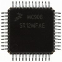
MC908SR12MFAE Freescale Semiconductor, MC908SR12MFAE Datasheet - Page 236

MC908SR12MFAE
Manufacturer Part Number
MC908SR12MFAE
Description
IC MCU 12K FLASH 8MHZ 48-LQFP
Manufacturer
Freescale Semiconductor
Series
HC08r
Datasheet
1.MC908SR12MFAE.pdf
(404 pages)
Specifications of MC908SR12MFAE
Core Processor
HC08
Core Size
8-Bit
Speed
8MHz
Connectivity
I²C, SCI
Peripherals
LVD, POR, PWM, Temp Sensor
Number Of I /o
31
Program Memory Size
12KB (12K x 8)
Program Memory Type
FLASH
Ram Size
512 x 8
Voltage - Supply (vcc/vdd)
4.5 V ~ 5.5 V
Data Converters
A/D 14x10b
Oscillator Type
Internal
Operating Temperature
-40°C ~ 125°C
Package / Case
48-LQFP
Lead Free Status / RoHS Status
Lead free / RoHS Compliant
Eeprom Size
-
Available stocks
Company
Part Number
Manufacturer
Quantity
Price
Company:
Part Number:
MC908SR12MFAE
Manufacturer:
Freescale Semiconductor
Quantity:
10 000
Company:
Part Number:
MC908SR12MFAER
Manufacturer:
Freescale Semiconductor
Quantity:
10 000
- Current page: 236 of 404
- Download datasheet (2Mb)
Analog-to-Digital Converter (ADC)
15.4.3 Conversion Time
Data Sheet
236
NOTE:
NOTE:
Conversion starts after a write to the ADSCR. One conversion will take
between 16 and 17 ADC clock cycles, therefore:
The ADC conversion time is determined by the clock source chosen and
the divide ratio selected. The clock source is either the bus clock or
CGMXCLK and is selectable by the ADICLK bit located in the ADC clock
register. The divide ratio is selected by the ADIV[2:0] bits.
For example, if a 4MHz CGMXCLK is selected as the ADC input clock
source, with a divide-by-four prescale, and the bus speed is set at 2MHz:
The ADC frequency must be between f
maximum to meet ADC specifications. (See
Characteristics.)
Since an ADC cycle may comprised of several bus cycles (two in the
previous example) and the start of a conversion is initiated by a bus cycle
write to the ADSCR, from zero to two additional bus cycles may occur
before the start of the initial ADC cycle. This results in a fractional ADC
cycle and is represented as the 17th cycle.
When OPOUT is selected as the ADC input, V
is the accumulation of the op-amp settling time and the normal ADC
conversion time. After writing to the ADSCR to initiate a conversion
cycle, the ADC module sends a signal to the analog module for a
OPOUT output. A signal will be sent back to the ADC by the analog
module to indicate that OPOUT signal is ready for sampling. Upon
receiving this signal, the ADC module starts its normal conversion cycle.
(See
Number of bus cycles = conversion time × bus frequency
Number of bus cycles = 16 µs × 2MHz = 32 to 34 cycles
24.12 5.0V ADC Electrical
Analog-to-Digital Converter (ADC)
Conversion time =
Conversion time =
MC68HC908SR12•MC68HC08SR12 — Rev. 5.0
16 to17 ADC cycles
16 to17 ADC cycles
Characteristics.)
ADC frequency
4MHz ÷ 4
ADIC
24.12 5.0V ADC Electrical
minimum and f
ADIN
Freescale Semiconductor
, the conversion time
= 16 to 17 µs
ADIC
Related parts for MC908SR12MFAE
Image
Part Number
Description
Manufacturer
Datasheet
Request
R
Part Number:
Description:
Manufacturer:
Freescale Semiconductor, Inc
Datasheet:
Part Number:
Description:
Manufacturer:
Freescale Semiconductor, Inc
Datasheet:
Part Number:
Description:
Manufacturer:
Freescale Semiconductor, Inc
Datasheet:
Part Number:
Description:
Manufacturer:
Freescale Semiconductor, Inc
Datasheet:
Part Number:
Description:
Manufacturer:
Freescale Semiconductor, Inc
Datasheet:
Part Number:
Description:
Manufacturer:
Freescale Semiconductor, Inc
Datasheet:
Part Number:
Description:
Manufacturer:
Freescale Semiconductor, Inc
Datasheet:
Part Number:
Description:
Manufacturer:
Freescale Semiconductor, Inc
Datasheet:
Part Number:
Description:
Manufacturer:
Freescale Semiconductor, Inc
Datasheet:
Part Number:
Description:
Manufacturer:
Freescale Semiconductor, Inc
Datasheet:
Part Number:
Description:
Manufacturer:
Freescale Semiconductor, Inc
Datasheet:
Part Number:
Description:
Manufacturer:
Freescale Semiconductor, Inc
Datasheet:
Part Number:
Description:
Manufacturer:
Freescale Semiconductor, Inc
Datasheet:
Part Number:
Description:
Manufacturer:
Freescale Semiconductor, Inc
Datasheet:
Part Number:
Description:
Manufacturer:
Freescale Semiconductor, Inc
Datasheet:


