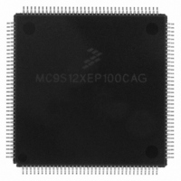
MC9S12XEP100CAG Freescale Semiconductor, MC9S12XEP100CAG Datasheet - Page 738

MC9S12XEP100CAG
Manufacturer Part Number
MC9S12XEP100CAG
Description
IC MCU 16BIT 1M FLASH 144-LQFP
Manufacturer
Freescale Semiconductor
Series
HCS12r
Datasheet
1.MC9S12XEP768CAL.pdf
(1328 pages)
Specifications of MC9S12XEP100CAG
Core Processor
HCS12X
Core Size
16-Bit
Speed
50MHz
Connectivity
CAN, EBI/EMI, I²C, IrDA, SCI, SPI
Peripherals
LVD, POR, PWM, WDT
Number Of I /o
119
Program Memory Size
1MB (1M x 8)
Program Memory Type
FLASH
Eeprom Size
4K x 8
Ram Size
64K x 8
Voltage - Supply (vcc/vdd)
1.72 V ~ 5.5 V
Data Converters
A/D 24x12b
Oscillator Type
External
Operating Temperature
-40°C ~ 85°C
Package / Case
144-LQFP
Processor Series
S12XE
Core
HCS12
Data Bus Width
16 bit
Data Ram Size
64 KB
Interface Type
CAN/SCI/SPI
Maximum Clock Frequency
50 MHz
Number Of Programmable I/os
119
Number Of Timers
25
Maximum Operating Temperature
+ 85 C
Mounting Style
SMD/SMT
3rd Party Development Tools
EWHCS12
Development Tools By Supplier
KIT33812ECUEVME, EVB9S12XEP100, DEMO9S12XEP100
Minimum Operating Temperature
- 40 C
On-chip Adc
24-ch x 12-bit
Cpu Family
HCS12X
Device Core Size
16b
Frequency (max)
50MHz
Total Internal Ram Size
64KB
# I/os (max)
119
Number Of Timers - General Purpose
25
Operating Supply Voltage (typ)
1.8/2.8/5V
Operating Supply Voltage (max)
1.98/2.9/5.5V
Operating Supply Voltage (min)
1.72/2.7/3.13V
Instruction Set Architecture
RISC
Operating Temp Range
-40C to 85C
Operating Temperature Classification
Industrial
Mounting
Surface Mount
Pin Count
144
Package Type
LQFP
Package
144LQFP
Family Name
HCS12X
Maximum Speed
50 MHz
Operating Supply Voltage
1.8|2.8|5 V
For Use With
EVB9S12XEP100 - BOARD EVAL FOR MC9S12XEP100DEMO9S12XEP100 - BOARD DEMO FOR MC9S12XEP100
Lead Free Status / RoHS Status
Lead free / RoHS Compliant
Available stocks
Company
Part Number
Manufacturer
Quantity
Price
Company:
Part Number:
MC9S12XEP100CAG
Manufacturer:
FREESCAL
Quantity:
244
Company:
Part Number:
MC9S12XEP100CAG
Manufacturer:
Freescale Semiconductor
Quantity:
10 000
- Current page: 738 of 1328
- Download datasheet (9Mb)
Chapter 20 Serial Communication Interface (S12SCIV5)
738
Because of an order from the United States International Trade Commission, BGA-packaged product lines and partnumbers
indicated here currently are not available from Freescale for import or sale in the United States prior to September 2010
Field
OR
NF
FE
PF
3
2
1
0
Overrun Flag — OR is set when software fails to read the SCI data register before the receive shift register
receives the next frame. The OR bit is set immediately after the stop bit has been completely received for the
second frame. The data in the shift register is lost, but the data already in the SCI data registers is not affected.
Clear OR by reading SCI status register 1 (SCISR1) with OR set and then reading SCI data register low
(SCIDRL).
0 No overrun
1 Overrun
Note: OR flag may read back as set when RDRF flag is clear. This may happen if the following sequence of
Noise Flag — NF is set when the SCI detects noise on the receiver input. NF bit is set during the same cycle as
the RDRF flag but does not get set in the case of an overrun. Clear NF by reading SCI status register 1(SCISR1),
and then reading SCI data register low (SCIDRL).
0 No noise
1 Noise
Framing Error Flag — FE is set when a logic 0 is accepted as the stop bit. FE bit is set during the same cycle
as the RDRF flag but does not get set in the case of an overrun. FE inhibits further data reception until it is
cleared. Clear FE by reading SCI status register 1 (SCISR1) with FE set and then reading the SCI data register
low (SCIDRL).
0 No framing error
1 Framing error
Parity Error Flag — PF is set when the parity enable bit (PE) is set and the parity of the received data does not
match the parity type bit (PT). PF bit is set during the same cycle as the RDRF flag but does not get set in the
case of an overrun. Clear PF by reading SCI status register 1 (SCISR1), and then reading SCI data register low
(SCIDRL).
0 No parity error
1 Parity error
events occurs:
Event 3 may be at exactly the same time as event 2 or any time after. When this happens, a dummy
SCIDRL read following event 4 will be required to clear the OR flag if further frames are to be received.
1. After the first frame is received, read status register SCISR1 (returns RDRF set and OR flag clear);
2. Receive second frame without reading the first frame in the data register (the second frame is not
3. Read data register SCIDRL (returns first frame and clears RDRF flag in the status register);
4. Read status register SCISR1 (returns RDRF clear and OR set).
received and OR flag is set);
Table 20-11. SCISR1 Field Descriptions (continued)
MC9S12XE-Family Reference Manual , Rev. 1.23
Description
Freescale Semiconductor
Related parts for MC9S12XEP100CAG
Image
Part Number
Description
Manufacturer
Datasheet
Request
R
Part Number:
Description:
Manufacturer:
Freescale Semiconductor, Inc
Datasheet:
Part Number:
Description:
Manufacturer:
Freescale Semiconductor, Inc
Datasheet:
Part Number:
Description:
Manufacturer:
Freescale Semiconductor, Inc
Datasheet:
Part Number:
Description:
Manufacturer:
Freescale Semiconductor, Inc
Datasheet:
Part Number:
Description:
Manufacturer:
Freescale Semiconductor, Inc
Datasheet:
Part Number:
Description:
Manufacturer:
Freescale Semiconductor, Inc
Datasheet:
Part Number:
Description:
Manufacturer:
Freescale Semiconductor, Inc
Datasheet:
Part Number:
Description:
Manufacturer:
Freescale Semiconductor, Inc
Datasheet:
Part Number:
Description:
Manufacturer:
Freescale Semiconductor, Inc
Datasheet:
Part Number:
Description:
Manufacturer:
Freescale Semiconductor, Inc
Datasheet:
Part Number:
Description:
Manufacturer:
Freescale Semiconductor, Inc
Datasheet:
Part Number:
Description:
Manufacturer:
Freescale Semiconductor, Inc
Datasheet:
Part Number:
Description:
Manufacturer:
Freescale Semiconductor, Inc
Datasheet:
Part Number:
Description:
Manufacturer:
Freescale Semiconductor, Inc
Datasheet:
Part Number:
Description:
Manufacturer:
Freescale Semiconductor, Inc
Datasheet:


