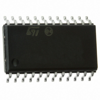
ST72F63BE2M1 STMicroelectronics, ST72F63BE2M1 Datasheet - Page 151

ST72F63BE2M1
Manufacturer Part Number
ST72F63BE2M1
Description
MCU 8BIT LS USB 8KB FLASH 24SOIC
Manufacturer
STMicroelectronics
Series
ST7r
Datasheet
1.ST72F63BD6U1TR.pdf
(186 pages)
Specifications of ST72F63BE2M1
Core Processor
ST7
Core Size
8-Bit
Speed
8MHz
Connectivity
I²C, SCI, USB
Peripherals
DMA, LVD, POR, PWM, WDT
Number Of I /o
14
Program Memory Size
8KB (8K x 8)
Program Memory Type
FLASH
Ram Size
1K x 8
Voltage - Supply (vcc/vdd)
4 V ~ 5.5 V
Oscillator Type
Internal
Operating Temperature
0°C ~ 70°C
Package / Case
24-SOIC (7.5mm Width)
Data Converters
A/D 12x10b
Processor Series
ST72F6x
Core
ST7
Data Bus Width
8 bit
Data Ram Size
384 B
Interface Type
I2C, SCI
Maximum Clock Frequency
8 MHz
Number Of Programmable I/os
14
Number Of Timers
1
Maximum Operating Temperature
+ 70 C
Mounting Style
SMD/SMT
Development Tools By Supplier
ST7MDTU3-EPB/US, ST7MDTULS-EVAL, ST72F63B-SK/RAIS, ST7MDTU3-EMU3, STX-RLINK
Minimum Operating Temperature
0 C
For Use With
497-8209 - BOARD EVAL USB STUSB02E/ST72F63B497-8208 - BOARD EVAL USB STUSB03E/ST72F63B497-5521 - EVAL BOARD LOW SPEED USB497-5046 - KIT TOOL FOR ST7/UPSD/STR7 MCU
Lead Free Status / RoHS Status
Lead free / RoHS Compliant
Eeprom Size
-
Lead Free Status / Rohs Status
Details
Other names
497-5624-5
Available stocks
Company
Part Number
Manufacturer
Quantity
Price
- Current page: 151 of 186
- Download datasheet (3Mb)
ST7263Bxx
Table 71.
1. The I
2. The I
3. The minimum V
Symbol
V
V
ports and control pins) must not exceed I
ports and control pins) must not exceed I
for ROM devices, min = V
OH
OL
(1)
(2)
IO
IO
current sourced must always respect the absolute maximum rating specified in
current sunk must always respect the absolute maximum rating specified in
Output low level voltage for a standard I/O pin
when up to 8 pins are sunk at the same time,
Port A0, Port A(3:7), Port C(0:2), Port D(0:7)
Output low level voltage for a high sink I/O pin
when up to 4 pins are sunk at the same time,
Port B(0:7)
Output low level voltage for a very high sink I/O
pin when up to 2 pins are sunk at the same
time, Port A1, Port A2
Output high level voltage for an I/O pin
when up to 8 pins are sourced at same time
Output driving current
Figure 63. V
OH
value (with I
DD
- 1.7 V
Parameter
OL
IO
=-10mA) depends on the chosen device type. For Flash devices, min = V
standard V
250
200
150
100
50
0
1
VSS
VDD
.
. True open drain I/O pins does not have V
DD
1.5
Doc ID 7516 Rev 8
=5 V
Vol_2mA (mV) at Vdd=5V
2
Iio (mA)
2.5
Conditions
I
I
I
I
I
IO
IO
IO
IO
IO
=+1.6 mA
=+10 mA
=+25 mA
=-10 mA
=-1.6 mA
3
Section 13.2
Section 13.2
OH
.
Electrical characteristics
V
3.5
V
DD
DD
and the sum of I
Min
-1.3
-
-
-
and the sum of I
-0.8
ai15597
(3)
4
DD
Max
0.4
1.3
1.5
- 1.3 V and
-
-
IO
IO
(I/O
151/186
(I/O
Unit
V
Related parts for ST72F63BE2M1
Image
Part Number
Description
Manufacturer
Datasheet
Request
R

Part Number:
Description:
KIT STARTER LOW COST ST7
Manufacturer:
STMicroelectronics
Datasheet:

Part Number:
Description:
LOW SPEED USB 8-BIT MCU FAMILY WITH FLASH/ROM, UP TO 512 BYTES RAM, 8-BIT ADC, WDG, TIMER, SCI & I�C
Manufacturer:
STMICROELECTRONICS [STMicroelectronics]
Datasheet:

Part Number:
Description:
STMicroelectronics [RIPPLE-CARRY BINARY COUNTER/DIVIDERS]
Manufacturer:
STMicroelectronics
Datasheet:

Part Number:
Description:
STMicroelectronics [LIQUID-CRYSTAL DISPLAY DRIVERS]
Manufacturer:
STMicroelectronics
Datasheet:

Part Number:
Description:
BOARD EVAL FOR MEMS SENSORS
Manufacturer:
STMicroelectronics
Datasheet:

Part Number:
Description:
NPN TRANSISTOR POWER MODULE
Manufacturer:
STMicroelectronics
Datasheet:

Part Number:
Description:
TURBOSWITCH ULTRA-FAST HIGH VOLTAGE DIODE
Manufacturer:
STMicroelectronics
Datasheet:

Part Number:
Description:
Manufacturer:
STMicroelectronics
Datasheet:

Part Number:
Description:
DIODE / SCR MODULE
Manufacturer:
STMicroelectronics
Datasheet:

Part Number:
Description:
DIODE / SCR MODULE
Manufacturer:
STMicroelectronics
Datasheet:

Part Number:
Description:
Search -----> STE16N100
Manufacturer:
STMicroelectronics
Datasheet:

Part Number:
Description:
Search ---> STE53NA50
Manufacturer:
STMicroelectronics
Datasheet:


