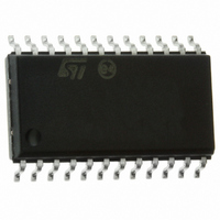
ST72F63BE2M1 STMicroelectronics, ST72F63BE2M1 Datasheet - Page 94

ST72F63BE2M1
Manufacturer Part Number
ST72F63BE2M1
Description
MCU 8BIT LS USB 8KB FLASH 24SOIC
Manufacturer
STMicroelectronics
Series
ST7r
Datasheet
1.ST72F63BD6U1TR.pdf
(186 pages)
Specifications of ST72F63BE2M1
Core Processor
ST7
Core Size
8-Bit
Speed
8MHz
Connectivity
I²C, SCI, USB
Peripherals
DMA, LVD, POR, PWM, WDT
Number Of I /o
14
Program Memory Size
8KB (8K x 8)
Program Memory Type
FLASH
Ram Size
1K x 8
Voltage - Supply (vcc/vdd)
4 V ~ 5.5 V
Oscillator Type
Internal
Operating Temperature
0°C ~ 70°C
Package / Case
24-SOIC (7.5mm Width)
Data Converters
A/D 12x10b
Processor Series
ST72F6x
Core
ST7
Data Bus Width
8 bit
Data Ram Size
384 B
Interface Type
I2C, SCI
Maximum Clock Frequency
8 MHz
Number Of Programmable I/os
14
Number Of Timers
1
Maximum Operating Temperature
+ 70 C
Mounting Style
SMD/SMT
Development Tools By Supplier
ST7MDTU3-EPB/US, ST7MDTULS-EVAL, ST72F63B-SK/RAIS, ST7MDTU3-EMU3, STX-RLINK
Minimum Operating Temperature
0 C
For Use With
497-8209 - BOARD EVAL USB STUSB02E/ST72F63B497-8208 - BOARD EVAL USB STUSB03E/ST72F63B497-5521 - EVAL BOARD LOW SPEED USB497-5046 - KIT TOOL FOR ST7/UPSD/STR7 MCU
Lead Free Status / RoHS Status
Lead free / RoHS Compliant
Eeprom Size
-
Lead Free Status / Rohs Status
Details
Other names
497-5624-5
Available stocks
Company
Part Number
Manufacturer
Quantity
Price
On-chip peripherals
94/186
Data register (SCIDR)
Reset value: Undefined
This register contains the received or transmitted data character, depending on whether it is
read from or written to.
The Data register performs a double function (read and write) since it is composed of two
registers, one for transmission (TDR) and one for reception (RDR).
The TDR register provides the parallel interface between the internal bus and the output
shift register (see
The RDR register provides the parallel interface between the input shift register and the
internal bus (see
DR7
7
DR6
Figure
Figure
2 RE Receiver enable.
1 RWU Receiver wakeup.
0 SBK Send break.
This bit enables the receiver. It is set and cleared by software.
0: Receiver is disabled
1: Receiver is enabled and begins searching for a start bit
This bit determines if the SCI is in mute mode or not. It is set and cleared by
software and can be cleared by hardware when a wakeup sequence is
recognized.
0: Receiver in Active mode
1: Receiver in Mute mode
Note: Before selecting Mute mode (setting the RWU bit), the SCI must
This bit set is used to send break characters. It is set and cleared by software.
0: No break character is transmitted
1: Break characters are transmitted
Note: If the SBK bit is set to “1” and then to “0”, the transmitter will send a
41).
41).
DR5
receive some data first, otherwise it cannot function in Mute mode with
wakeup by idle line detection.
BREAK word at the end of the current word.
Doc ID 7516 Rev 8
DR4
Read/write
DR3
DR2
DR1
ST7263Bxx
DR0
0


