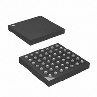
ATXMEGA32A4-CUR Atmel, ATXMEGA32A4-CUR Datasheet - Page 162

ATXMEGA32A4-CUR
Manufacturer Part Number
ATXMEGA32A4-CUR
Description
MCU AVR 32+4 FLASH 49VFBGA
Manufacturer
Atmel
Series
AVR® XMEGAr
Specifications of ATXMEGA32A4-CUR
Core Processor
AVR
Core Size
8/16-Bit
Speed
32MHz
Connectivity
I²C, IrDA, SPI, UART/USART
Peripherals
Brown-out Detect/Reset, DMA, POR, PWM, WDT
Number Of I /o
34
Program Memory Size
32KB (16K x 16)
Program Memory Type
FLASH
Eeprom Size
2K x 8
Ram Size
4K x 8
Voltage - Supply (vcc/vdd)
1.6 V ~ 3.6 V
Data Converters
A/D 12x12b, D/A 2x12b
Oscillator Type
Internal
Operating Temperature
-40°C ~ 85°C
Package / Case
49-VFBGA
For Use With
ATAVRONEKIT - KIT AVR/AVR32 DEBUGGER/PROGRMMRATSTK600 - DEV KIT FOR AVR/AVR32770-1007 - ISP 4PORT ATMEL AVR MCU SPI/JTAG770-1004 - ISP 4PORT FOR ATMEL AVR MCU SPI
Lead Free Status / RoHS Status
Lead free / RoHS Compliant
Available stocks
Company
Part Number
Manufacturer
Quantity
Price
- Current page: 162 of 445
- Download datasheet (6Mb)
14.8.5
8077H–AVR–12/09
Port override for Waveform Generation
Figure 14-14. Dual-slope Pulse Width Modulation
Using dual-slope PWM result in a lower maximum operation frequency compared to the single-
slope PWM operation.
The period register (PER) defines the PWM resolution. The minimum resolution is 2-bit
(PER=0x0003), and maximum resolution is 16-bit (PER=MAX).
The following equation can be used for calculate the exact resolution for dual-slope PWM
(R
The PWM frequency depends on the period setting (PER) and the Peripheral Clock frequency
(f
N represents the prescaler divider used (1, 2, 4, 8, 64, 256, 1024, or event channel n).
To make the waveform generation available on the port pins the corresponding port pin direction
must be set as output. The Timer/Counter will override the port pin values when the CC channel
is enabled (CCENx) and a waveform generation mode is selected.
Figure 14-15 on page 163
1, CC channel A to D will override port pin 0 to 3 output value (OUTxn) on the corresponding
port pin (Pxn). For Timer/Counter 1, CC channel A and B will override port pin 4 and 5. Enabling
inverted I/O on the port pin (INVENxn) inverts the corresponding WG output.
R
f
PWM_DS
PER
PWM_DS
PWM_DS
CNT
WG Output
), and can be calculated by the following equation:
=
):
=
------------------- -
2NPER
log
---------------------------------- -
f
PER
MAX
TOP
BOT
(
log
PER
2 ( )
+
1
)
shows the port override for Timer/Counter 0 and 1. For Timer/Counter
CCx
Period (T)
CCx=BOT
CCx=TOP
XMEGA A
"update"
"match"
162
Related parts for ATXMEGA32A4-CUR
Image
Part Number
Description
Manufacturer
Datasheet
Request
R

Part Number:
Description:
DEV KIT FOR AVR/AVR32
Manufacturer:
Atmel
Datasheet:

Part Number:
Description:
INTERVAL AND WIPE/WASH WIPER CONTROL IC WITH DELAY
Manufacturer:
ATMEL Corporation
Datasheet:

Part Number:
Description:
Low-Voltage Voice-Switched IC for Hands-Free Operation
Manufacturer:
ATMEL Corporation
Datasheet:

Part Number:
Description:
MONOLITHIC INTEGRATED FEATUREPHONE CIRCUIT
Manufacturer:
ATMEL Corporation
Datasheet:

Part Number:
Description:
AM-FM Receiver IC U4255BM-M
Manufacturer:
ATMEL Corporation
Datasheet:

Part Number:
Description:
Monolithic Integrated Feature Phone Circuit
Manufacturer:
ATMEL Corporation
Datasheet:

Part Number:
Description:
Multistandard Video-IF and Quasi Parallel Sound Processing
Manufacturer:
ATMEL Corporation
Datasheet:

Part Number:
Description:
High-performance EE PLD
Manufacturer:
ATMEL Corporation
Datasheet:

Part Number:
Description:
8-bit Flash Microcontroller
Manufacturer:
ATMEL Corporation
Datasheet:

Part Number:
Description:
2-Wire Serial EEPROM
Manufacturer:
ATMEL Corporation
Datasheet:


