ATXMEGA32A4-CUR Atmel, ATXMEGA32A4-CUR Datasheet - Page 296
ATXMEGA32A4-CUR
Manufacturer Part Number
ATXMEGA32A4-CUR
Description
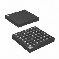
MCU AVR 32+4 FLASH 49VFBGA
Manufacturer
Atmel
Series
AVR® XMEGAr
Specifications of ATXMEGA32A4-CUR
Core Processor
AVR
Core Size
8/16-Bit
Speed
32MHz
Connectivity
I²C, IrDA, SPI, UART/USART
Peripherals
Brown-out Detect/Reset, DMA, POR, PWM, WDT
Number Of I /o
34
Program Memory Size
32KB (16K x 16)
Program Memory Type
FLASH
Eeprom Size
2K x 8
Ram Size
4K x 8
Voltage - Supply (vcc/vdd)
1.6 V ~ 3.6 V
Data Converters
A/D 12x12b, D/A 2x12b
Oscillator Type
Internal
Operating Temperature
-40°C ~ 85°C
Package / Case
49-VFBGA
For Use With
ATAVRONEKIT - KIT AVR/AVR32 DEBUGGER/PROGRMMRATSTK600 - DEV KIT FOR AVR/AVR32770-1007 - ISP 4PORT ATMEL AVR MCU SPI/JTAG770-1004 - ISP 4PORT FOR ATMEL AVR MCU SPI
Lead Free Status / RoHS Status
Lead free / RoHS Compliant
Available stocks
Company
Part Number
Manufacturer
Quantity
Price


25.7
25.8
25.9
8077H–AVR–12/09
Compare function
Starting a conversion
ADC Clock and Conversion Timing
Figure 25-11. Unsigned single ended and internal input, input range, and result representation
The ADC has a built in 12-bit compare function. The ADC compare register can hold a 12-bit
value that represent an analog threshold voltage. Each ADC Channel can be configured to auto-
matically compare its result with this 12-bit compare value to give an interrupt or event only
when the result is above or below the threshold.
All four ADC Channels share the same compare register.
Before a conversion is started, the desired input source must be selected for one or more ADC
channels. An ADC conversion for a ADC channel can either be started by the application soft-
ware writing to the start conversion bit for the ADC channel, or from any of the events in the
Event System. It is possible to write the start conversion bit for several ADC channels at the
same time, or to use one event to trigger conversions on several ADC channels at the same
time. Using this it is possible to scan several or all ADC channels from one event.
The ADC is clocked from the Peripheral Clock. The ADC can prescale the Peripheral Clock to
provide an ADC Clock (Clk
Figure 25-12. ADC Prescaler
The maximum ADC sample rate is given by the he ADC clock frequency (f
sample a new measurement on every ADC clock cycle.
The propagation delay of an ADC measurement is given by:
Sample Rate
VREF
GND
−
Δ
V
=
f
ADC
PRESCALER[2:0]
ADC
Clk
) that is within the minimum and maximum frequency for the ADC.
PER
VINN
=
VREF
2
VINP
−
Δ
9-bit ADC Prescaler
V
4095
4094
4093
Dec
203
202
201
200
...
...
0
Clk
FFD
0CB
0CA
Hex
FFF
FFE
0C9
0C8
...
ADC
0
1111 1111 1111
1111 1111 1110
1111 1111 1101
0000 1100 1011
0000 1100 1010
0000 1100 1001
0000 1100 1000
0000 0000 0000
Binary
...
0000 1111 1111 1111
0000 1111 1111 1110
0000 1111 1111 1101
0000 0000 1100 1011
0000 0000 1100 1010
0000 0000 1100 1001
0000 0000 1100 1000
0000 0000 0000 0000
16-bit result register
ADC
XMEGA A
). The ADC can
...
296
Related parts for ATXMEGA32A4-CUR
Image
Part Number
Description
Manufacturer
Datasheet
Request
R

Part Number:
Description:
DEV KIT FOR AVR/AVR32
Manufacturer:
Atmel
Datasheet:

Part Number:
Description:
INTERVAL AND WIPE/WASH WIPER CONTROL IC WITH DELAY
Manufacturer:
ATMEL Corporation
Datasheet:
Part Number:
Description:
Low-Voltage Voice-Switched IC for Hands-Free Operation
Manufacturer:
ATMEL Corporation
Datasheet:
Part Number:
Description:
MONOLITHIC INTEGRATED FEATUREPHONE CIRCUIT
Manufacturer:
ATMEL Corporation
Datasheet:
Part Number:
Description:
AM-FM Receiver IC U4255BM-M
Manufacturer:
ATMEL Corporation
Datasheet:
Part Number:
Description:
Monolithic Integrated Feature Phone Circuit
Manufacturer:
ATMEL Corporation
Datasheet:
Part Number:
Description:
Multistandard Video-IF and Quasi Parallel Sound Processing
Manufacturer:
ATMEL Corporation
Datasheet:
Part Number:
Description:
High-performance EE PLD
Manufacturer:
ATMEL Corporation
Datasheet:
Part Number:
Description:
8-bit Flash Microcontroller
Manufacturer:
ATMEL Corporation
Datasheet:
Part Number:
Description:
2-Wire Serial EEPROM
Manufacturer:
ATMEL Corporation
Datasheet: