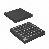
ATXMEGA32A4-CUR Atmel, ATXMEGA32A4-CUR Datasheet - Page 375

ATXMEGA32A4-CUR
Manufacturer Part Number
ATXMEGA32A4-CUR
Description
MCU AVR 32+4 FLASH 49VFBGA
Manufacturer
Atmel
Series
AVR® XMEGAr
Specifications of ATXMEGA32A4-CUR
Core Processor
AVR
Core Size
8/16-Bit
Speed
32MHz
Connectivity
I²C, IrDA, SPI, UART/USART
Peripherals
Brown-out Detect/Reset, DMA, POR, PWM, WDT
Number Of I /o
34
Program Memory Size
32KB (16K x 16)
Program Memory Type
FLASH
Eeprom Size
2K x 8
Ram Size
4K x 8
Voltage - Supply (vcc/vdd)
1.6 V ~ 3.6 V
Data Converters
A/D 12x12b, D/A 2x12b
Oscillator Type
Internal
Operating Temperature
-40°C ~ 85°C
Package / Case
49-VFBGA
For Use With
ATAVRONEKIT - KIT AVR/AVR32 DEBUGGER/PROGRMMRATSTK600 - DEV KIT FOR AVR/AVR32770-1007 - ISP 4PORT ATMEL AVR MCU SPI/JTAG770-1004 - ISP 4PORT FOR ATMEL AVR MCU SPI
Lead Free Status / RoHS Status
Lead free / RoHS Compliant
Available stocks
Company
Part Number
Manufacturer
Quantity
Price
- Current page: 375 of 445
- Download datasheet (6Mb)
30.11.4
30.11.4.1
8077H–AVR–12/09
EEPROM Programming
Addressing the EEPROM
1.
2.
3.
during self-programming.
The result will be available in the NVM DATA0 register. The CPU is halted during the complete
execution of the command.
The EEPROM can be read and written from application code in any part of the Flash. Its is both
byte and page accessible. This means that either one byte or one page can be written to the
EEPROM at once. One byte is read from the EEPROM during read.
The EEPROM can be accessed through the NVM controller (I/O mapped), similar to the Flash
Program memory, or it can be memory mapped into the Data Memory space to be accessed
similar to SRAM.
When accessing the EEPROM through the NVM Controller, the NVM Address (ADDR) register
is used to address the EEPROM, while the NVM Data (DATA) register is used to store or load
EEPROM data.
For EEPROM page programming the ADDR register can be treated as having two section. The
least significant bits address the bytes within a page, while the most significant bits address the
page within the EEPROM. This is shown in
page (E2BYTE) is held by the bits [1:BYTEMSB] in the ADDR register. The remaining bits
[PAGEMSB:BYTEMSB+1] in the ADDR register holds the EEPROM page address (E2PAGE).
Together E2BYTE and E2PAGE holds an absolute address to a byte in the EEPROM. The size
of E2WORD and E2PAGE will depend on the page and flash size in the device, refer to the
device data sheet for details on this.
Load the NVM ADDR registers with the address to the fuse byte to read.
Load the NVM CMD register with the Read Fuses command.
Set the CMDEX bit in the NVM CTRLA register. This requires the timed CCP sequence
Figure 30-3 on page
376. The byte address in the
XMEGA A
375
Related parts for ATXMEGA32A4-CUR
Image
Part Number
Description
Manufacturer
Datasheet
Request
R

Part Number:
Description:
DEV KIT FOR AVR/AVR32
Manufacturer:
Atmel
Datasheet:

Part Number:
Description:
INTERVAL AND WIPE/WASH WIPER CONTROL IC WITH DELAY
Manufacturer:
ATMEL Corporation
Datasheet:

Part Number:
Description:
Low-Voltage Voice-Switched IC for Hands-Free Operation
Manufacturer:
ATMEL Corporation
Datasheet:

Part Number:
Description:
MONOLITHIC INTEGRATED FEATUREPHONE CIRCUIT
Manufacturer:
ATMEL Corporation
Datasheet:

Part Number:
Description:
AM-FM Receiver IC U4255BM-M
Manufacturer:
ATMEL Corporation
Datasheet:

Part Number:
Description:
Monolithic Integrated Feature Phone Circuit
Manufacturer:
ATMEL Corporation
Datasheet:

Part Number:
Description:
Multistandard Video-IF and Quasi Parallel Sound Processing
Manufacturer:
ATMEL Corporation
Datasheet:

Part Number:
Description:
High-performance EE PLD
Manufacturer:
ATMEL Corporation
Datasheet:

Part Number:
Description:
8-bit Flash Microcontroller
Manufacturer:
ATMEL Corporation
Datasheet:

Part Number:
Description:
2-Wire Serial EEPROM
Manufacturer:
ATMEL Corporation
Datasheet:


