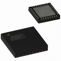
AT89C5131A-PUTUM Atmel, AT89C5131A-PUTUM Datasheet - Page 31

AT89C5131A-PUTUM
Manufacturer Part Number
AT89C5131A-PUTUM
Description
IC 8051 MCU FLASH 32K USB 32QFN
Manufacturer
Atmel
Series
AT89C513xr
Datasheet
1.AT89C5130A-PUTUM.pdf
(188 pages)
Specifications of AT89C5131A-PUTUM
Core Processor
C52X2
Core Size
8-Bit
Speed
48MHz
Connectivity
I²C, SPI, UART/USART, USB
Peripherals
LED, POR, PWM, WDT
Number Of I /o
18
Program Memory Size
32KB (32K x 8)
Program Memory Type
FLASH
Eeprom Size
4K x 8
Ram Size
1.25K x 8
Voltage - Supply (vcc/vdd)
2.7 V ~ 5.5 V
Oscillator Type
Internal
Operating Temperature
-40°C ~ 85°C
Package / Case
32-VQFN Exposed Pad, 32-HVQFN, 32-SQFN, 32-DHVQFN
Core
8051
Processor Series
AT89x
Data Bus Width
8 bit
Maximum Clock Frequency
48 MHz
Data Ram Size
1.25 KB
Number Of Programmable I/os
34
Number Of Timers
16 bit
Operating Supply Voltage
2.7 V to 5.5 V
Mounting Style
SMD/SMT
Height
0.95 mm
Interface Type
2-Wire, EUART, SPI, USB
Length
7 mm
Maximum Operating Temperature
+ 85 C
Minimum Operating Temperature
- 40 C
Supply Voltage (max)
5.5 V
Supply Voltage (min)
2.7 V
Width
7 mm
For Use With
AT89OCD-01 - USB EMULATOR FOR AT8XC51 MCUAT89STK-10 - KIT EVAL APPL MASS STORAGEAT89STK-05 - KIT STARTER FOR AT89C5131
Lead Free Status / RoHS Status
Lead free / RoHS Compliant
Data Converters
-
Lead Free Status / Rohs Status
Details
Available stocks
Company
Part Number
Manufacturer
Quantity
Price
Part Number:
AT89C5131A-PUTUM
Manufacturer:
ATMEL/爱特梅尔
Quantity:
20 000
- Current page: 31 of 188
- Download datasheet (2Mb)
8.2
Figure 8-4.
8.2.1
8.2.1.1
8.2.1.2
8.2.1.3
4337K–USB–04/08
3FFFh for
AT89C5130A
for 16 KB
7FFFh for
AT89C5131A
for 32 KB
Hardware Security (1 Byte)
Flash Memory Architecture
Column Latches (128 Bytes)
FM0 Memory Architecture
User Space
Extra Row (XRow)
Hardware Security Space
Extra Row (128 Bytes)
Flash Memory Architecture
AT89C5130A/31A-M features two on-chip Flash memories:
The FM0 supports both parallel programming and Serial In-System Programming (ISP) whereas
FM1 supports only parallel programming by programmers. The ISP mode is detailed in the “In-
System Programming” section.
All Read/Write access operations on Flash memory by user application are managed by a set of
API described in the “In-System Programming” section.
The Flash memory is made up of 4 blocks (see Figure 8-4):
This space is composed of a 16/32 Kbytes Flash memory organized in 128/256 pages of 128
bytes. It contains the user’s application code.
This row is a part of FM0 and has a size of 128 bytes. The extra row contains information for
bootloader usage (see
The hardware security space is a part of FM0 and has a size of 1 byte.
The 4 MSB can be read/written by software. The 4 LSB can only be read by software and written
by hardware in parallel mode.
• Flash memory FM0:
• Flash memory FM1:
1. The memory array (user space) 32 Kbytes
2. The Extra Row
3. The Hardware security bits
4. The column latch registers
containing 32 Kbytes of program memory (user space) organized into 128-byte pages,
3 Kbytes for bootloader and Application Programming Interfaces (API).
0000h
Flash Memory
User Space
16/32 KB
FM0
9-3 “Software Registers” on page
FM1 mapped between FFFFh and
F400h when bit ENBOOT is set in
AUXR1 register
Flash Memory
Boot Space
3 Kbytes
FM1
AT89C5130A/31A-M
41)
FFFFh
F400h
31
Related parts for AT89C5131A-PUTUM
Image
Part Number
Description
Manufacturer
Datasheet
Request
R

Part Number:
Description:
Manufacturer:
Atmel Corporation
Datasheet:

Part Number:
Description:
Manufacturer:
Atmel Corporation
Datasheet:

Part Number:
Description:
IC 8051 MCU FLASH 32K USB 52PLCC
Manufacturer:
Atmel
Datasheet:

Part Number:
Description:
IC MCU 32KB 3-3.6V USB 48-VQFN
Manufacturer:
Atmel
Datasheet:

Part Number:
Description:
MCU 8051 32K FLASH USB 28-SOIC
Manufacturer:
Atmel
Datasheet:

Part Number:
Description:
IC 8051 MCU FLASH 32K USB 64VQFP
Manufacturer:
Atmel
Datasheet:

Part Number:
Description:
MCU 8051 32K FLASH USB 64-VQFP
Manufacturer:
Atmel
Datasheet:

Part Number:
Description:
MCU 8051 32K FLASH USB 28-SOIC
Manufacturer:
Atmel
Datasheet:

Part Number:
Description:
MCU 8051 32K FLASH USB 52-PLCC
Manufacturer:
Atmel
Datasheet:

Part Number:
Description:
IC 8051 MCU FLASH 32K USB 48QFN
Manufacturer:
Atmel
Datasheet:

Part Number:
Description:
IC 8051 MCU FLASH 32K USB 64VQFP
Manufacturer:
Atmel
Datasheet:

Part Number:
Description:
IC 8051 MCU FLASH 32K USB 32QFN
Manufacturer:
Atmel
Datasheet:

Part Number:
Description:
IC 8051 MCU FLASH 32K USB 52PLCC
Manufacturer:
Atmel
Datasheet:

Part Number:
Description:
IC 8051 MCU FLASH 32K USB 28SOIC
Manufacturer:
Atmel
Datasheet:


