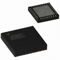
AT89C5131A-PUTUM Atmel, AT89C5131A-PUTUM Datasheet - Page 32

AT89C5131A-PUTUM
Manufacturer Part Number
AT89C5131A-PUTUM
Description
IC 8051 MCU FLASH 32K USB 32QFN
Manufacturer
Atmel
Series
AT89C513xr
Datasheet
1.AT89C5130A-PUTUM.pdf
(188 pages)
Specifications of AT89C5131A-PUTUM
Core Processor
C52X2
Core Size
8-Bit
Speed
48MHz
Connectivity
I²C, SPI, UART/USART, USB
Peripherals
LED, POR, PWM, WDT
Number Of I /o
18
Program Memory Size
32KB (32K x 8)
Program Memory Type
FLASH
Eeprom Size
4K x 8
Ram Size
1.25K x 8
Voltage - Supply (vcc/vdd)
2.7 V ~ 5.5 V
Oscillator Type
Internal
Operating Temperature
-40°C ~ 85°C
Package / Case
32-VQFN Exposed Pad, 32-HVQFN, 32-SQFN, 32-DHVQFN
Core
8051
Processor Series
AT89x
Data Bus Width
8 bit
Maximum Clock Frequency
48 MHz
Data Ram Size
1.25 KB
Number Of Programmable I/os
34
Number Of Timers
16 bit
Operating Supply Voltage
2.7 V to 5.5 V
Mounting Style
SMD/SMT
Height
0.95 mm
Interface Type
2-Wire, EUART, SPI, USB
Length
7 mm
Maximum Operating Temperature
+ 85 C
Minimum Operating Temperature
- 40 C
Supply Voltage (max)
5.5 V
Supply Voltage (min)
2.7 V
Width
7 mm
For Use With
AT89OCD-01 - USB EMULATOR FOR AT8XC51 MCUAT89STK-10 - KIT EVAL APPL MASS STORAGEAT89STK-05 - KIT STARTER FOR AT89C5131
Lead Free Status / RoHS Status
Lead free / RoHS Compliant
Data Converters
-
Lead Free Status / Rohs Status
Details
Available stocks
Company
Part Number
Manufacturer
Quantity
Price
Part Number:
AT89C5131A-PUTUM
Manufacturer:
ATMEL/爱特梅尔
Quantity:
20 000
- Current page: 32 of 188
- Download datasheet (2Mb)
8.2.1.4
8.3
8.3.1
8.3.2
32
Overview of FM0 Operations
AT89C5130A/31A-M
Mapping of the Memory Space
Launching Programming
Column Latches
The column latches, also part of FM0, have a size of full page (128 bytes).
The column latches are the entrance buffers of the three previous memory locations (user array,
XRow and Hardware security byte).
The CPU interfaces to the Flash memory through the FCON register and AUXR1 register.
These registers are used to:
By default, the user space is accessed by MOVC instruction for read only. The column latches
space is made accessible by setting the FPS bit in FCON register. Writing is possible from
0000h to 3FFFH/7FFFh, address bits 6 to 0 are used to select an address within a page while
bits 14 to 7 are used to select the programming address of the page.
Setting this bit takes precedence on the EXTRAM bit in AUXR register.
The other memory spaces (user, extra row, hardware security) are made accessible in the code
segment by programming bits FMOD0 and FMOD1 in FCON register in accordance with
Table 8-2. A MOVC instruction is then used for reading these spaces.
Table 8-2.
FPL3:0 bits in FCON register are used to secure the launch of programming. A specific
sequence must be written in these bits to unlock the write protection and to launch the program-
ming. This sequence is 5 followed by A. Table 8-3 summarizes the memory spaces to program
according to FMOD1:0 bits.
• Map the memory spaces in the adressable space
• Launch the programming of the memory spaces
• Get the status of the Flash memory (busy/not busy)
• Select the Flash memory FM0/FM1.
FMOD1
FM0 Blocks Select Bits
0
0
1
1
FMOD0
0
1
0
1
FM0 Adressable Space
User (0000h-FFFFh)
Extra Row(FF80h-FFFFh)
Hardware Security (0000h)
reserved
4337K–USB–04/08
Related parts for AT89C5131A-PUTUM
Image
Part Number
Description
Manufacturer
Datasheet
Request
R

Part Number:
Description:
Manufacturer:
Atmel Corporation
Datasheet:

Part Number:
Description:
Manufacturer:
Atmel Corporation
Datasheet:

Part Number:
Description:
IC 8051 MCU FLASH 32K USB 52PLCC
Manufacturer:
Atmel
Datasheet:

Part Number:
Description:
IC MCU 32KB 3-3.6V USB 48-VQFN
Manufacturer:
Atmel
Datasheet:

Part Number:
Description:
MCU 8051 32K FLASH USB 28-SOIC
Manufacturer:
Atmel
Datasheet:

Part Number:
Description:
IC 8051 MCU FLASH 32K USB 64VQFP
Manufacturer:
Atmel
Datasheet:

Part Number:
Description:
MCU 8051 32K FLASH USB 64-VQFP
Manufacturer:
Atmel
Datasheet:

Part Number:
Description:
MCU 8051 32K FLASH USB 28-SOIC
Manufacturer:
Atmel
Datasheet:

Part Number:
Description:
MCU 8051 32K FLASH USB 52-PLCC
Manufacturer:
Atmel
Datasheet:

Part Number:
Description:
IC 8051 MCU FLASH 32K USB 48QFN
Manufacturer:
Atmel
Datasheet:

Part Number:
Description:
IC 8051 MCU FLASH 32K USB 64VQFP
Manufacturer:
Atmel
Datasheet:

Part Number:
Description:
IC 8051 MCU FLASH 32K USB 32QFN
Manufacturer:
Atmel
Datasheet:

Part Number:
Description:
IC 8051 MCU FLASH 32K USB 52PLCC
Manufacturer:
Atmel
Datasheet:

Part Number:
Description:
IC 8051 MCU FLASH 32K USB 28SOIC
Manufacturer:
Atmel
Datasheet:


