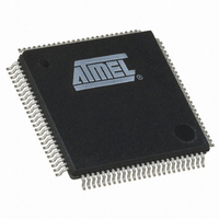
AT91SAM7X128B-AU Atmel, AT91SAM7X128B-AU Datasheet - Page 184

AT91SAM7X128B-AU
Manufacturer Part Number
AT91SAM7X128B-AU
Description
IC MCU 128KB FLASH 100LQFP
Manufacturer
Atmel
Series
AT91SAMr
Specifications of AT91SAM7X128B-AU
Core Processor
ARM7
Core Size
16/32-Bit
Speed
55MHz
Connectivity
CAN, Ethernet, I²C, SPI, SSC, UART/USART, USB
Peripherals
Brown-out Detect/Reset, DMA, POR, PWM, WDT
Number Of I /o
62
Program Memory Size
128KB (128K x 8)
Program Memory Type
FLASH
Ram Size
32K x 8
Voltage - Supply (vcc/vdd)
1.65 V ~ 1.95 V
Data Converters
A/D 8x10b
Oscillator Type
Internal
Operating Temperature
-40°C ~ 85°C
Package / Case
100-LQFP
Processor Series
AT91SAMx
Core
ARM7TDMI
Data Bus Width
32 bit
Data Ram Size
32 KB
Interface Type
JTAG, SPI, UART
Maximum Clock Frequency
55 MHz
Number Of Timers
1
Maximum Operating Temperature
+ 85 C
Mounting Style
SMD/SMT
3rd Party Development Tools
JTRACE-ARM-2M, KSK-AT91SAM7X-PL, MDK-ARM, RL-ARM, ULINK2
Development Tools By Supplier
AT91SAM-ICE, AT91-ISP, AT91SAM7X-EK
Minimum Operating Temperature
- 40 C
On-chip Adc
10 bit, 8 Channel
Controller Family/series
AT91SAM7xxxxx
No. Of I/o's
62
Ram Memory Size
32KB
Cpu Speed
55MHz
No. Of Timers
1
Rohs Compliant
Yes
Cpu Family
91S
Device Core
ARM7TDMI
Device Core Size
32b
Frequency (max)
55MHz
Total Internal Ram Size
32KB
# I/os (max)
62
Number Of Timers - General Purpose
3
Operating Supply Voltage (typ)
1.8/3.3V
Operating Supply Voltage (max)
1.95/3.6V
Operating Supply Voltage (min)
1.65/3V
Instruction Set Architecture
RISC
Operating Temp Range
-40C to 85C
Operating Temperature Classification
Industrial
Mounting
Surface Mount
Pin Count
100
Package Type
LQFP
Lead Free Status / RoHS Status
Lead free / RoHS Compliant
Eeprom Size
-
Lead Free Status / Rohs Status
Lead free / RoHS Compliant
Available stocks
Company
Part Number
Manufacturer
Quantity
Price
Company:
Part Number:
AT91SAM7X128B-AU
Manufacturer:
Atmel
Quantity:
1 929
Part Number:
AT91SAM7X128B-AU
Manufacturer:
ATMEL/爱特梅尔
Quantity:
20 000
- Current page: 184 of 687
- Download datasheet (11Mb)
184
SAM7X512/256/128 Preliminary
3. Setting PLL and divider:
4. Selection of Master Clock and Processor Clock
All parameters needed to configure PLL and the divider are located in the CKGR_PLLR
register.
The DIV field is used to control divider itself. A value between 0 and 255 can be pro-
grammed. Divider output is divider input divided by DIV parameter. By default DIV
parameter is set to 0 which means that divider is turned off.
The OUT field is used to select the PLL B output frequency range.
The MUL field is the PLL multiplier factor. This parameter can be programmed between 0
and 2047. If MUL is set to 0, PLL will be turned off, otherwise the PLL output frequency is
PLL input frequency multiplied by (MUL + 1).
The PLLCOUNT field specifies the number of slow clock cycles before LOCK bit is set in the
PMC_SR register after CKGR_PLLR register has been written.
Once the PMC_PLL register has been written, the user must wait for the LOCK bit to be set
in the PMC_SR register. This can be done either by polling the status register or by waiting
the interrupt line to be raised if the associated interrupt to LOCK has been enabled in the
PMC_IER register. All parameters in CKGR_PLLR can be programmed in a single write
operation. If at some stage one of the following parameters, MUL, DIV is modified, LOCK bit
will go low to indicate that PLL is not ready yet. When PLL is locked, LOCK will be set again.
The user is constrained to wait for LOCK bit to be set before using the PLL output clock.
The USBDIV field is used to control the additional divider by 1, 2 or 4, which generates the
USB clock(s).
Code Example:
If PLL and divider are enabled, the PLL input clock is the main clock. PLL output clock is PLL
input clock multiplied by 5. Once CKGR_PLLR has been written, LOCK bit will be set after
eight slow clock cycles.
The Master Clock and the Processor Clock are configurable via the PMC_MCKR register.
The CSS field is used to select the Master Clock divider source. By default, the selected
clock source is slow clock.
The PRES field is used to control the Master Clock prescaler. The user can choose between
different values (1, 2, 4, 8, 16, 32, 64). Master Clock output is prescaler input divided by
PRES parameter. By default, PRES parameter is set to 1 which means that master clock is
equal to slow clock.
Once the PMC_MCKR register has been written, the user must wait for the MCKRDY bit to
be set in the PMC_SR register. This can be done either by polling the status register or by
waiting for the interrupt line to be raised if the associated interrupt to MCKRDY has been
enabled in the PMC_IER register.
The PMC_MCKR register must not be programmed in a single write operation. The pre-
ferred programming sequence for the PMC_MCKR register is as follows:
write_register(CKGR_PLLR,0x00040805)
6120I–ATARM–06-Apr-11
Related parts for AT91SAM7X128B-AU
Image
Part Number
Description
Manufacturer
Datasheet
Request
R

Part Number:
Description:
KIT EVAL FOR AT91SAM7X256/128
Manufacturer:
Atmel
Datasheet:

Part Number:
Description:
MCU, MPU & DSP Development Tools KICKSTART KIT ATMEL AT91SAM7X
Manufacturer:
IAR Systems

Part Number:
Description:
MCU ARM9 64K SRAM 144-LFBGA
Manufacturer:
Atmel
Datasheet:

Part Number:
Description:
IC ARM7 MCU FLASH 256K 100LQFP
Manufacturer:
Atmel
Datasheet:

Part Number:
Description:
IC ARM9 MPU 217-LFBGA
Manufacturer:
Atmel
Datasheet:

Part Number:
Description:
MCU ARM9 ULTRA LOW PWR 217-LFBGA
Manufacturer:
Atmel
Datasheet:

Part Number:
Description:
MCU ARM9 324-TFBGA
Manufacturer:
Atmel
Datasheet:

Part Number:
Description:
IC MCU ARM9 SAMPLING 217CBGA
Manufacturer:
Atmel
Datasheet:

Part Number:
Description:
IC ARM9 MCU 217-LFBGA
Manufacturer:
Atmel
Datasheet:

Part Number:
Description:
IC ARM9 MCU 208-PQFP
Manufacturer:
Atmel
Datasheet:

Part Number:
Description:
MCU ARM 512K HS FLASH 100-LQFP
Manufacturer:
Atmel
Datasheet:

Part Number:
Description:
MCU ARM 512K HS FLASH 100-TFBGA
Manufacturer:
Atmel
Datasheet:

Part Number:
Description:
IC ARM9 MCU 200 MHZ 324-TFBGA
Manufacturer:
Atmel
Datasheet:

Part Number:
Description:
IC ARM MCU 16BIT 128K 256BGA
Manufacturer:
Atmel
Datasheet:

Part Number:
Description:
IC ARM7 MCU 32BIT 128K 64LQFP
Manufacturer:
Atmel
Datasheet:


