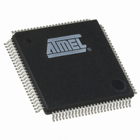
AT91SAM7X128B-AU Atmel, AT91SAM7X128B-AU Datasheet - Page 360

AT91SAM7X128B-AU
Manufacturer Part Number
AT91SAM7X128B-AU
Description
IC MCU 128KB FLASH 100LQFP
Manufacturer
Atmel
Series
AT91SAMr
Specifications of AT91SAM7X128B-AU
Core Processor
ARM7
Core Size
16/32-Bit
Speed
55MHz
Connectivity
CAN, Ethernet, I²C, SPI, SSC, UART/USART, USB
Peripherals
Brown-out Detect/Reset, DMA, POR, PWM, WDT
Number Of I /o
62
Program Memory Size
128KB (128K x 8)
Program Memory Type
FLASH
Ram Size
32K x 8
Voltage - Supply (vcc/vdd)
1.65 V ~ 1.95 V
Data Converters
A/D 8x10b
Oscillator Type
Internal
Operating Temperature
-40°C ~ 85°C
Package / Case
100-LQFP
Processor Series
AT91SAMx
Core
ARM7TDMI
Data Bus Width
32 bit
Data Ram Size
32 KB
Interface Type
JTAG, SPI, UART
Maximum Clock Frequency
55 MHz
Number Of Timers
1
Maximum Operating Temperature
+ 85 C
Mounting Style
SMD/SMT
3rd Party Development Tools
JTRACE-ARM-2M, KSK-AT91SAM7X-PL, MDK-ARM, RL-ARM, ULINK2
Development Tools By Supplier
AT91SAM-ICE, AT91-ISP, AT91SAM7X-EK
Minimum Operating Temperature
- 40 C
On-chip Adc
10 bit, 8 Channel
Controller Family/series
AT91SAM7xxxxx
No. Of I/o's
62
Ram Memory Size
32KB
Cpu Speed
55MHz
No. Of Timers
1
Rohs Compliant
Yes
Cpu Family
91S
Device Core
ARM7TDMI
Device Core Size
32b
Frequency (max)
55MHz
Total Internal Ram Size
32KB
# I/os (max)
62
Number Of Timers - General Purpose
3
Operating Supply Voltage (typ)
1.8/3.3V
Operating Supply Voltage (max)
1.95/3.6V
Operating Supply Voltage (min)
1.65/3V
Instruction Set Architecture
RISC
Operating Temp Range
-40C to 85C
Operating Temperature Classification
Industrial
Mounting
Surface Mount
Pin Count
100
Package Type
LQFP
Lead Free Status / RoHS Status
Lead free / RoHS Compliant
Eeprom Size
-
Lead Free Status / Rohs Status
Lead free / RoHS Compliant
Available stocks
Company
Part Number
Manufacturer
Quantity
Price
Company:
Part Number:
AT91SAM7X128B-AU
Manufacturer:
Atmel
Quantity:
1 929
Part Number:
AT91SAM7X128B-AU
Manufacturer:
ATMEL/爱特梅尔
Quantity:
20 000
- Current page: 360 of 687
- Download datasheet (11Mb)
31.6.5
31.6.5.1
31.6.5.2
31.6.6
360
SAM7X512/256/128 Preliminary
Frame Sync
Receive Compare Modes
Frame Sync Data
Frame Sync Edge Detection
The Transmitter and Receiver Frame Sync pins, TF and RF, can be programmed to generate
different kinds of frame synchronization signals. The Frame Sync Output Selection (FSOS) field
in the Receive Frame Mode Register (SSC_RFMR) and in the Transmit Frame Mode Register
(SSC_TFMR) are used to select the required waveform.
If a pulse waveform is selected, the Frame Sync Length (FSLEN) field in SSC_RFMR and
SSC_TFMR programs the length of the pulse, from 1 bit time up to 16 bit time.
The periodicity of the Receive and Transmit Frame Sync pulse output can be programmed
through the Period Divider Selection (PERIOD) field in SSC_RCMR and SSC_TCMR.
Frame Sync Data transmits or receives a specific tag during the Frame Sync signal.
During the Frame Sync signal, the Receiver can sample the RD line and store the data in the
Receive Sync Holding Register and the transmitter can transfer Transmit Sync Holding Register
in the Shifter Register. The data length to be sampled/shifted out during the Frame Sync signal
is programmed by the FSLEN field in SSC_RFMR/SSC_TFMR and has a maximum value of 16.
Concerning the Receive Frame Sync Data operation, if the Frame Sync Length is equal to or
lower than the delay between the start event and the actual data reception, the data sampling
operation is performed in the Receive Sync Holding Register through the Receive Shift Register.
The Transmit Frame Sync Operation is performed by the transmitter only if the bit Frame Sync
Data Enable (FSDEN) in SSC_TFMR is set. If the Frame Sync length is equal to or lower than
the delay between the start event and the actual data transmission, the normal transmission has
priority and the data contained in the Transmit Sync Holding Register is transferred in the Trans-
mit Register, then shifted out.
T h e F r a m e S y n c E d g e d e t e c t i o n i s p r o g r a m m e d b y t h e F S E D G E f i e l d i n
SSC_RFMR/SSC_TFMR. This sets the corresponding flags RXSYN/TXSYN in the SSC Status
Register (SSC_SR) on frame synchro edge detection (signals RF/TF).
Figure 31-12. Receive Compare Modes
• Programmable low or high levels during data transfer are supported.
• Programmable high levels before the start of data transfers or toggling are also supported.
(Input)
RD
RK
CMP0
(4 in This Example)
CMP1
Up to 16 Bits
FSLEN
CMP2
CMP3
Start
Ignored
STDLY
B0
DATLEN
B1
6120I–ATARM–06-Apr-11
B2
Related parts for AT91SAM7X128B-AU
Image
Part Number
Description
Manufacturer
Datasheet
Request
R

Part Number:
Description:
KIT EVAL FOR AT91SAM7X256/128
Manufacturer:
Atmel
Datasheet:

Part Number:
Description:
MCU, MPU & DSP Development Tools KICKSTART KIT ATMEL AT91SAM7X
Manufacturer:
IAR Systems

Part Number:
Description:
MCU ARM9 64K SRAM 144-LFBGA
Manufacturer:
Atmel
Datasheet:

Part Number:
Description:
IC ARM7 MCU FLASH 256K 100LQFP
Manufacturer:
Atmel
Datasheet:

Part Number:
Description:
IC ARM9 MPU 217-LFBGA
Manufacturer:
Atmel
Datasheet:

Part Number:
Description:
MCU ARM9 ULTRA LOW PWR 217-LFBGA
Manufacturer:
Atmel
Datasheet:

Part Number:
Description:
MCU ARM9 324-TFBGA
Manufacturer:
Atmel
Datasheet:

Part Number:
Description:
IC MCU ARM9 SAMPLING 217CBGA
Manufacturer:
Atmel
Datasheet:

Part Number:
Description:
IC ARM9 MCU 217-LFBGA
Manufacturer:
Atmel
Datasheet:

Part Number:
Description:
IC ARM9 MCU 208-PQFP
Manufacturer:
Atmel
Datasheet:

Part Number:
Description:
MCU ARM 512K HS FLASH 100-LQFP
Manufacturer:
Atmel
Datasheet:

Part Number:
Description:
MCU ARM 512K HS FLASH 100-TFBGA
Manufacturer:
Atmel
Datasheet:

Part Number:
Description:
IC ARM9 MCU 200 MHZ 324-TFBGA
Manufacturer:
Atmel
Datasheet:

Part Number:
Description:
IC ARM MCU 16BIT 128K 256BGA
Manufacturer:
Atmel
Datasheet:

Part Number:
Description:
IC ARM7 MCU 32BIT 128K 64LQFP
Manufacturer:
Atmel
Datasheet:


