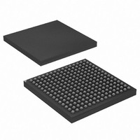
AT91CAP7E-NA-ZJ Atmel, AT91CAP7E-NA-ZJ Datasheet - Page 189

AT91CAP7E-NA-ZJ
Manufacturer Part Number
AT91CAP7E-NA-ZJ
Description
MCU CAP7 FPGA 225LFBGA
Manufacturer
Atmel
Series
CAP™r
Specifications of AT91CAP7E-NA-ZJ
Core Processor
ARM7
Core Size
16/32-Bit
Speed
80MHz
Connectivity
EBI/EMI, FPGA, IrDA, SPI, UART/USART, USB
Peripherals
DMA, POR, PWM, WDT
Number Of I /o
32
Program Memory Size
256KB (256K x 8)
Program Memory Type
ROM
Ram Size
160K x 8
Voltage - Supply (vcc/vdd)
1.08 V ~ 1.32 V
Data Converters
A/D 8x10b
Oscillator Type
Internal
Operating Temperature
-40°C ~ 85°C
Package / Case
225-LFBGA
Processor Series
AT91Mx
Core
ARM7TDMI
Data Bus Width
32 bit
3rd Party Development Tools
JTRACE-ARM-2M, MDK-ARM, RL-ARM, ULINK2
Lead Free Status / RoHS Status
Lead free / RoHS Compliant
Eeprom Size
-
Lead Free Status / Rohs Status
Details
Available stocks
Company
Part Number
Manufacturer
Quantity
Price
- Current page: 189 of 520
- Download datasheet (11Mb)
• TRC: Row Cycle Delay
Reset value is seven cycles.
This field defines the delay between a Refresh and an Activate Command in number of cycles. Number of cycles is
between 0 and 15.
• TRP: Row Precharge Delay
Reset value is three cycles.
This field defines the delay between a Precharge Command and another Command in number of cycles. Number of cycles
is between 0 and 15.
• TRCD: Row to Column Delay
Reset value is two cycles.
This field defines the delay between an Activate Command and a Read/Write Command in number of cycles. Number of
cycles is between 0 and 15.
• TRAS: Active to Precharge Delay
Reset value is five cycles.
This field defines the delay between an Activate Command and a Precharge Command in number of cycles. Number of
cycles is between 0 and 15.
• TXSR: Exit Self Refresh to Active Delay
Reset value is eight cycles.
This field defines the delay between SCKE set high and an Activate Command in number of cycles. Number of cycles is
between 0 and 15.
22.7.4
Register Name:
Access Type:
• DA: Decode Cycle Enable
A decode cycle can be added on the addresses as soon as a non-sequential access is performed on the AHB bus.
The addition of the decode cycle allows the SDRAMC to gain time to access the SDRAM memory.
0: Decode cycle is disabled.
1: Decode cycle is enabled.
8549A–CAP–10/08
31
23
15
–
–
–
7
–
SDRAMC High Speed Register
30
22
14
–
–
–
6
–
29
21
13
–
–
–
5
–
SDRAMC_HSR
Read/Write
28
20
12
–
–
–
4
–
27
19
11
–
–
–
3
–
26
18
10
–
–
–
2
–
25
17
–
–
9
–
1
–
AT91CAP7E
DA
24
16
–
–
8
–
0
189
Related parts for AT91CAP7E-NA-ZJ
Image
Part Number
Description
Manufacturer
Datasheet
Request
R

Part Number:
Description:
Customizable Microcontroller
Manufacturer:
ATMEL Corporation
Datasheet:

Part Number:
Description:
DEV KIT FOR AVR/AVR32
Manufacturer:
Atmel
Datasheet:

Part Number:
Description:
INTERVAL AND WIPE/WASH WIPER CONTROL IC WITH DELAY
Manufacturer:
ATMEL Corporation
Datasheet:

Part Number:
Description:
Low-Voltage Voice-Switched IC for Hands-Free Operation
Manufacturer:
ATMEL Corporation
Datasheet:

Part Number:
Description:
MONOLITHIC INTEGRATED FEATUREPHONE CIRCUIT
Manufacturer:
ATMEL Corporation
Datasheet:

Part Number:
Description:
AM-FM Receiver IC U4255BM-M
Manufacturer:
ATMEL Corporation
Datasheet:

Part Number:
Description:
Monolithic Integrated Feature Phone Circuit
Manufacturer:
ATMEL Corporation
Datasheet:

Part Number:
Description:
Multistandard Video-IF and Quasi Parallel Sound Processing
Manufacturer:
ATMEL Corporation
Datasheet:

Part Number:
Description:
High-performance EE PLD
Manufacturer:
ATMEL Corporation
Datasheet:

Part Number:
Description:
8-bit Flash Microcontroller
Manufacturer:
ATMEL Corporation
Datasheet:

Part Number:
Description:
2-Wire Serial EEPROM
Manufacturer:
ATMEL Corporation
Datasheet:


