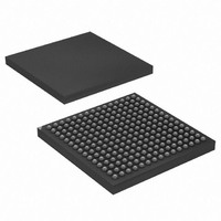
AT91CAP7E-NA-ZJ Atmel, AT91CAP7E-NA-ZJ Datasheet - Page 447

AT91CAP7E-NA-ZJ
Manufacturer Part Number
AT91CAP7E-NA-ZJ
Description
MCU CAP7 FPGA 225LFBGA
Manufacturer
Atmel
Series
CAP™r
Specifications of AT91CAP7E-NA-ZJ
Core Processor
ARM7
Core Size
16/32-Bit
Speed
80MHz
Connectivity
EBI/EMI, FPGA, IrDA, SPI, UART/USART, USB
Peripherals
DMA, POR, PWM, WDT
Number Of I /o
32
Program Memory Size
256KB (256K x 8)
Program Memory Type
ROM
Ram Size
160K x 8
Voltage - Supply (vcc/vdd)
1.08 V ~ 1.32 V
Data Converters
A/D 8x10b
Oscillator Type
Internal
Operating Temperature
-40°C ~ 85°C
Package / Case
225-LFBGA
Processor Series
AT91Mx
Core
ARM7TDMI
Data Bus Width
32 bit
3rd Party Development Tools
JTRACE-ARM-2M, MDK-ARM, RL-ARM, ULINK2
Lead Free Status / RoHS Status
Lead free / RoHS Compliant
Eeprom Size
-
Lead Free Status / Rohs Status
Details
Available stocks
Company
Part Number
Manufacturer
Quantity
Price
- Current page: 447 of 520
- Download datasheet (11Mb)
31.6
WARNING: The UDP peripheral clock in the Power Management Controller (PMC) must be enabled before any read/write
operations to the UDP registers including the UDP_TXVC register.
Table 31-4.
Notes:
8549A–CAP–10/08
Offset
0x000
0x004
0x008
0x00C
0x010
0x014
0x018
0x01C
0x020
0x024
0x028
0x02C
0x030
.
.
.
See Note:
0x050
.
.
.
See Note:
0x070
0x074
0x078 - 0xFC
USB Device Port (UDP) User Interface
1. The addresses of the UDP_ CSRx registers are calculated as: 0x030 + 4(Endpoint Number - 1).
2. The addresses of the UDP_ FDRx registers are calculated as: 0x050 + 4(Endpoint Number - 1).
3. See Warning above the
(1)
(2)
UDP Memory Map
Register
Frame Number Register
Global State Register
Function Address Register
Reserved
Interrupt Enable Register
Interrupt Disable Register
Interrupt Mask Register
Interrupt Status Register
Interrupt Clear Register
Reserved
Reset Endpoint Register
Reserved
Endpoint 0 Control and Status Register
.
.
.
Endpoint
Endpoint 0 FIFO Data Register
.
.
.
Endpoint
Reserved
Transceiver Control Register
Reserved
5
5
Control and Status Register
FIFO Data Register
”UDP Memory Map”
on this page.
Name
UDP_ FRM_NUM
UDP_ GLB_STAT
UDP_ FADDR
–
UDP_ IER
UDP_ IDR
UDP_ IMR
UDP_ ISR
UDP_ ICR
–
UDP_ RST_EP
–
UDP_CSR0
UDP_CSR5
UDP_ FDR0
UDP_
–
UDP_ TXVC
–
FDR5
(3)
Access
Read
Read/Write
Read/Write
–
Write
Write
Read
Read
Write
–
Read/Write
–
Read/Write
Read/Write
Read/Write
Read/Write
–
Read/Write
–
AT91CAP7E
0x0000_0000
0x0000_0100
0x0000_1200
Reset State
0x0000_0000
–
0x0000_XX00
–
–
0x0000_0000
0x0000_0000
0x0000_0000
0x0000_0000
–
0x0000_0100
–
447
Related parts for AT91CAP7E-NA-ZJ
Image
Part Number
Description
Manufacturer
Datasheet
Request
R

Part Number:
Description:
Customizable Microcontroller
Manufacturer:
ATMEL Corporation
Datasheet:

Part Number:
Description:
DEV KIT FOR AVR/AVR32
Manufacturer:
Atmel
Datasheet:

Part Number:
Description:
INTERVAL AND WIPE/WASH WIPER CONTROL IC WITH DELAY
Manufacturer:
ATMEL Corporation
Datasheet:

Part Number:
Description:
Low-Voltage Voice-Switched IC for Hands-Free Operation
Manufacturer:
ATMEL Corporation
Datasheet:

Part Number:
Description:
MONOLITHIC INTEGRATED FEATUREPHONE CIRCUIT
Manufacturer:
ATMEL Corporation
Datasheet:

Part Number:
Description:
AM-FM Receiver IC U4255BM-M
Manufacturer:
ATMEL Corporation
Datasheet:

Part Number:
Description:
Monolithic Integrated Feature Phone Circuit
Manufacturer:
ATMEL Corporation
Datasheet:

Part Number:
Description:
Multistandard Video-IF and Quasi Parallel Sound Processing
Manufacturer:
ATMEL Corporation
Datasheet:

Part Number:
Description:
High-performance EE PLD
Manufacturer:
ATMEL Corporation
Datasheet:

Part Number:
Description:
8-bit Flash Microcontroller
Manufacturer:
ATMEL Corporation
Datasheet:

Part Number:
Description:
2-Wire Serial EEPROM
Manufacturer:
ATMEL Corporation
Datasheet:


