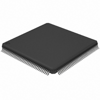
LH75411N0Q100C0;55 NXP Semiconductors, LH75411N0Q100C0;55 Datasheet - Page 37

LH75411N0Q100C0;55
Manufacturer Part Number
LH75411N0Q100C0;55
Description
IC ARM7 BLUESTREAK MCU 144LQFP
Manufacturer
NXP Semiconductors
Series
BlueStreak ; LH7r
Datasheet
1.LH75401N0Q100C055.pdf
(63 pages)
Specifications of LH75411N0Q100C0;55
Package / Case
144-LQFP
Core Processor
ARM7
Core Size
16/32-Bit
Speed
84MHz
Connectivity
EBI/EMI, SPI, SSI, SSP, UART/USART
Peripherals
Brown-out Detect/Reset, DMA, LCD, POR, PWM, WDT
Number Of I /o
76
Program Memory Type
ROMless
Ram Size
32K x 8
Voltage - Supply (vcc/vdd)
1.7 V ~ 3.6 V
Data Converters
A/D 8x10b
Oscillator Type
External
Operating Temperature
-40°C ~ 85°C
Processor Series
LH75
Core
ARM7TDMI-S
Data Bus Width
32 bit
Data Ram Size
32 KB
Interface Type
JTAG, SPI, UART
Maximum Clock Frequency
84 MHz
Number Of Programmable I/os
76
Number Of Timers
3
Operating Supply Voltage
3.3 V
Maximum Operating Temperature
+ 85 C
Mounting Style
SMD/SMT
3rd Party Development Tools
MDK-ARM, RL-ARM, ULINK2
Minimum Operating Temperature
- 40 C
On-chip Adc
10 bit, 8 Channel
Lead Free Status / RoHS Status
Lead free / RoHS Compliant
Eeprom Size
-
Program Memory Size
-
Lead Free Status / Rohs Status
Lead free / RoHS Compliant
Other names
568-4330
935285046557
935285046557
System-on-Chip
Analog-To-Digital Converter Electrical
Characteristics
extended temperature operation. See Figure 6 for the
ADC transfer characteristics.
NOTES:
1. The analog section of the ADC takes 16 × A2DCLK cycles per conversion,
2. The internal voltage reference is driven to nominal value VREF = 2.0 V. Using the Reference Multiplexer,
3. The analog input pins can be driven anywhere between the power supply rails. If the voltage at the input to the
4. Bandgap and other low-bandwidth circuitry operating. All other ADC blocks shut down.
Preliminary data sheet
A/D Resolution
Throughput Conversion
Acquisition Time
Clk Period
Differential Non-Linearity
Integral Non-Linearity
Offset Error
Gain Error
On-chip Voltage Reference (VREF)
Negative Reference Input (VREF-)
Positive Reference Input (VREF+)
Crosstalk between channels
Analog Input Voltage Range
Analog Input Current
Reference Input Current
Analog input capacitance
Operating Supply Voltage
Operating Current, VDDA
Standby Current
Stop Current, VDDA
Brown Out Trip Point
Brown Out Hysterisis
Operating Temperature
Table 21 shows the derated specifications for
plus 1 × A2DCLK cycles to be made available in the PCLK domain.
An additional 3 × PCLK cycles are required before being available on the APB.
alternative low impedance (RS < 500) voltages can be selected as reference voltages. The range of voltages
allowed are specified above. However, the on-chip reference cannot drive the ADC unless the reference buffer is switched on.
ADC exceeds VREF+ or is below VREF-, the A/D result will saturate appropriately at positive or negative full scale.
Trying to pull the analog input pins above or below the power supply rails will cause protection diodes to be
forward-biased, resulting in large current source/sink and possible damage to the ADC.
PARAMETER
Table 21. ADC Electrical Characteristics at Industrial Operating Range
(VREF-) +1.0
NXP Semiconductors
VSSA
Rev. 01 — 16 July 2007
-0.99
MIN.
1.85
-3.5
-4.0
500
−40
-35
3.0
10
17
3
0
VSSA
VREF
TYP.
2.63
590
180
120
-60
< 1
2.0
(VREF+) -1.0
VDDA
VDDA
MAX.
5,000
+3.5
2.15
+35
4.5
4.0
3.6
10
15
85
5
5
CLK Cycles
CLK Cycles
UNITS
LSB
LSB
LSB
Bits
mV
mV
dB
µA
µA
µA
µA
µA
pF
°C
ns
V
V
V
V
V
V
LH75401/LH75411
NOTES
2
1
2
3
4
37


