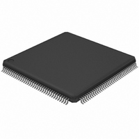
LH75411N0Q100C0;55 NXP Semiconductors, LH75411N0Q100C0;55 Datasheet - Page 40

LH75411N0Q100C0;55
Manufacturer Part Number
LH75411N0Q100C0;55
Description
IC ARM7 BLUESTREAK MCU 144LQFP
Manufacturer
NXP Semiconductors
Series
BlueStreak ; LH7r
Datasheet
1.LH75401N0Q100C055.pdf
(63 pages)
Specifications of LH75411N0Q100C0;55
Package / Case
144-LQFP
Core Processor
ARM7
Core Size
16/32-Bit
Speed
84MHz
Connectivity
EBI/EMI, SPI, SSI, SSP, UART/USART
Peripherals
Brown-out Detect/Reset, DMA, LCD, POR, PWM, WDT
Number Of I /o
76
Program Memory Type
ROMless
Ram Size
32K x 8
Voltage - Supply (vcc/vdd)
1.7 V ~ 3.6 V
Data Converters
A/D 8x10b
Oscillator Type
External
Operating Temperature
-40°C ~ 85°C
Processor Series
LH75
Core
ARM7TDMI-S
Data Bus Width
32 bit
Data Ram Size
32 KB
Interface Type
JTAG, SPI, UART
Maximum Clock Frequency
84 MHz
Number Of Programmable I/os
76
Number Of Timers
3
Operating Supply Voltage
3.3 V
Maximum Operating Temperature
+ 85 C
Mounting Style
SMD/SMT
3rd Party Development Tools
MDK-ARM, RL-ARM, ULINK2
Minimum Operating Temperature
- 40 C
On-chip Adc
10 bit, 8 Channel
Lead Free Status / RoHS Status
Lead free / RoHS Compliant
Eeprom Size
-
Program Memory Size
-
Lead Free Status / Rohs Status
Lead free / RoHS Compliant
Other names
568-4330
935285046557
935285046557
LH75401/LH75411
AC Characteristics
point of the signal.
NOTE: The values in Table 24 represent the timing with no internal arbitration
40
D[15:0]
D[15:0]
D[15:0]
nCS3 - nCS0
nCS3 -nCS0
nOE
nOE
nBLE1 - nBLE0 Out 30 pF
nBLE1 - nBLE0 Out 30 pF
nBLE1 - nBLE0 Out 30 pF
nWE
nWE
nWAIT
SSPFRM
SIGNAL
All signal transitions are measured from the 50 %
SSPRX
SSPTX
PARAMETER
SIGNAL
tRSTOV
tOSC32
tOSC14
tPORH
tLREG
delay and 1 wait state memory access. This is the worst case (fastest) timing.
Out
Out
I/O
In
Out 50 pF
Out 50 pF
Out 30 pF
Out 30 pF
Out 30 pF
Out 30 pF
Out 30 pF
Out 30 pF
I/O LOAD PARAMETER
In
In
Linear regulator stabilization time after power-up
Oscillator stabilization time after Power Up (VDDC = VDDCMIN)
Oscillator stabilization time after Power Up (VDDC = VDDCMIN)
nPOR LOW to nPOR valid (once sampled LOW)
nPOR hold extend to allow PLL to lock once XTAL is stable
LOAD
50 pF
50 pF
PARAMETER
tOVSSPFRM
tOHBEW
tOHBER
tIVWAIT
tOVSSPTX
tOHWE
tOVWE
tOVCS
tOHCS
tOVOE
tOHOE
tOVBE
tOVD
tOHD
tISSPRX
tIDD
Table 24. Memory Interface Signals
Table 25. Synchronous Serial Port
Table 26. Power-up Stabilization
3 × tHCLK – 6 ns
3 × tHCLK – 6 ns
3 × tHCLK – 6 ns
3 × tHCLK – 6 ns
2 × tHCLK – 6 ns
2 × tHCLK – 6 ns 2 tHCLK – 2.2 ns nWE output invalid following address valid
NXP Semiconductors
Rev. 01 — 16 July 2007
DESCRIPTION
MINIMUM
22 ns
MIN.
MAX.
14 ns SSPFRM output valid, referenced to SSPCLK
12 ns SSPTX output valid, referenced to SSPCLK
2 tHCLK – 18 ns nWAIT input valid following address valid
2 tHCLK – 18 ns Data input valid following address valid
2 × tHCLK – 18 ns
tHCLK + 10 ns
tHCLK + 10 ns
tHCLK + 10 ns
tHCLK + 8 ns
tHCLK + 6 ns
+ (nWAIT –1)
MAXIMUM
SSPRX input valid, referenced to SSPCLK
× tHCLK
Data output invalid following address valid
Data output valid following address valid
Data Input Valid, following
Address Valid (nWAIT states)
nCS output valid following address valid
nCS output invalid following address valid
nOE output valid following address valid
nOE output invalid following address valid
nBLE output valid following address valid
nBLE output invalid following address
valid, read cycle
nBLE output invalid following address
valid, write cycle
nWE output valid following address valid
COMMENT
COMMENTS
TYP.
Preliminary data sheet
3.5
System-on-Chip
MAX.
200
550
2.5
10
HCLK
UNIT
ms
ms
µs
µs


