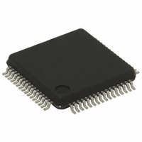
ST72F321BAR6T6 STMicroelectronics, ST72F321BAR6T6 Datasheet - Page 89

ST72F321BAR6T6
Manufacturer Part Number
ST72F321BAR6T6
Description
MCU 8BIT 32KB FLASH/ROM 64-LQFP
Manufacturer
STMicroelectronics
Series
ST7r
Datasheet
1.ST72F321BK6T6.pdf
(187 pages)
Specifications of ST72F321BAR6T6
Core Processor
ST7
Core Size
8-Bit
Speed
8MHz
Connectivity
I²C, SCI, SPI
Peripherals
LVD, POR, PWM, WDT
Number Of I /o
48
Program Memory Size
32KB (32K x 8)
Program Memory Type
FLASH
Ram Size
1K x 8
Voltage - Supply (vcc/vdd)
3.8 V ~ 5.5 V
Data Converters
A/D 16x10b
Oscillator Type
Internal
Operating Temperature
-40°C ~ 85°C
Package / Case
64-LQFP
Processor Series
ST72F3x
Core
ST7
Data Bus Width
8 bit
Data Ram Size
1 KB
Interface Type
I2C, SCI, SPI
Maximum Clock Frequency
8 MHz
Number Of Programmable I/os
48
Number Of Timers
2
Maximum Operating Temperature
+ 85 C
Mounting Style
SMD/SMT
Development Tools By Supplier
ST7232X-EVAL, ST7232X-SK/RAIS, ST72321B-D/RAIS, ST7MDT20-DVP3, ST7MDT20J-EMU3, ST7MDT20M-EMU3, STX-RLINK
Minimum Operating Temperature
- 40 C
On-chip Adc
10 bit, 16 Channel
For Use With
497-5046 - KIT TOOL FOR ST7/UPSD/STR7 MCU
Lead Free Status / RoHS Status
Lead free / RoHS Compliant
Eeprom Size
-
Lead Free Status / Rohs Status
Details
Other names
497-5582
Available stocks
Company
Part Number
Manufacturer
Quantity
Price
Company:
Part Number:
ST72F321BAR6T6
Manufacturer:
STMicroelectronics
Quantity:
10 000
SERIAL PERIPHERAL INTERFACE (Cont’d)
10.5.3.1 Functional Description
A basic example of interconnections between a
single master and a single slave is illustrated in
Figure
The MOSI pins are connected together and the
MISO pins are connected together. In this way
data is transferred serially between master and
slave (most significant bit first).
Figure 55. Single Master/ Single Slave Application
– SS: Slave select:
This input signal acts as a ‘chip select’ to let
the SPI master communicate with slaves indi-
vidually and to avoid contention on the data
lines. Slave SS inputs can be driven by stand-
ard I/O ports on the master MCU.
55.
MSBit
8-BIT SHIFT REGISTER
GENERATOR
CLOCK
SPI
MASTER
LSBit
ST72321BRx, ST72321BARx ST72321BJx, ST72321BKx
SCK
MOSI
SS
MISO
+5V
The communication is always initiated by the mas-
ter. When the master device transmits data to a
slave device via MOSI pin, the slave device re-
sponds by sending data to the master device via
the MISO pin. This implies full duplex communica-
tion with both data out and data in synchronized
with the same clock signal (which is provided by
the master device via the SCK pin).
To use a single data line, the MISO and MOSI pins
must be connected at each node ( in this case only
simplex communication is possible).
Four possible data/clock timing relationships may
be chosen (see
must be programmed with the same timing mode.
MISO
MOSI
SCK
SS
Figure
8-BIT SHIFT REGISTER
MSBit
Not used if SS is managed
by software
58) but master and slave
SLAVE
LSBit
89/187


