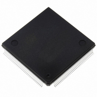
ST10F269Z2Q6 STMicroelectronics, ST10F269Z2Q6 Datasheet - Page 125

ST10F269Z2Q6
Manufacturer Part Number
ST10F269Z2Q6
Description
MCU 16BIT 256K FLASH 144PQFP
Manufacturer
STMicroelectronics
Series
ST10r
Specifications of ST10F269Z2Q6
Core Processor
ST10
Core Size
16-Bit
Speed
40MHz
Connectivity
CAN, EBI/EMI, SSC, UART/USART
Peripherals
POR, PWM, WDT
Number Of I /o
111
Program Memory Size
256KB (256K x 8)
Program Memory Type
FLASH
Ram Size
12K x 8
Voltage - Supply (vcc/vdd)
4.5 V ~ 5.5 V
Data Converters
A/D 16x10b
Oscillator Type
Internal
Operating Temperature
-40°C ~ 85°C
Package / Case
144-QFP
Controller Family/series
ST10
No. Of I/o's
111
Ram Memory Size
12KB
Cpu Speed
40MHz
No. Of Timers
5
Embedded Interface Type
CAN, SSC, USART
Rohs Compliant
Yes
Processor Series
ST10F26x
Core
ST10
Data Bus Width
16 bit
Data Ram Size
12 KB
Interface Type
CAN, SSC, USART
Maximum Clock Frequency
40 MHz
Number Of Programmable I/os
111
Number Of Timers
2 x 16 bit
Operating Supply Voltage
0.3 V to 4 V
Maximum Operating Temperature
+ 85 C
Mounting Style
SMD/SMT
Minimum Operating Temperature
- 40 C
On-chip Adc
16 bit x 10 bit
Lead Free Status / RoHS Status
Lead free / RoHS Compliant
Eeprom Size
-
Lead Free Status / Rohs Status
Details
Other names
497-4833
Available stocks
Company
Part Number
Manufacturer
Quantity
Price
Company:
Part Number:
ST10F269Z2Q6
Manufacturer:
ST
Quantity:
201
Company:
Part Number:
ST10F269Z2Q6
Manufacturer:
ST
Quantity:
745
Company:
Part Number:
ST10F269Z2Q6
Manufacturer:
STMicroelectronics
Quantity:
10 000
Part Number:
ST10F269Z2Q6
Manufacturer:
ST
Quantity:
20 000
BUSCON0 (FF0Ch / 86h)
BUSCON1 (FF14h / 8Ah)
BUSCON2 (FF16h / 8Bh)
BUSCON3 (FF18h / 8Ch)
WRCFG
CLKEN
BYTDIS
ROMEN
SGTDIS
ROMS1
STKSZ
CSWEN0 CSREN0 RDYPOL0 RDYEN0
CSWEN1 CSREN1 RDYPOL1 RDYEN1
CSWEN2 CSREN2 RDYPOL2 RDYEN2
CSWEN3 CSREN3 RDYPOL3 RDYEN3
RW
RW
RW
RW
15
15
15
15
RW
RW
RW
RW
14
14
14
14
Write Configuration Control (Inverted copy of bit WRC of RP0H)
‘0’: Pins WR and BHE retain their normal function
‘1’: Pin WR acts as WRL, pin BHE acts as WRH.
System Clock Output Enable (CLKOUT)
‘0’: CLKOUT disabled: pin may be used for general purpose I/O
‘1’: CLKOUT enabled: pin outputs the system clock signal.
Disable/Enable Control for Pin BHE (Set according to data bus width)
‘0’: Pin BHE enabled
‘1’: Pin BHE disabled, pin may be used for general purpose I/O.
Internal Memory Enable (Set according to pin EA during reset)
‘0’: Internal Memory disabled: accesses to the Memory area use the external bus
‘1’: Internal Memory enabled.
Segmentation Disable/Enable Control
‘0’: Segmentation enabled (CSP is saved/restored during interrupt entry/exit)
‘1’: Segmentation disabled (Only IP is saved/restored).
Internal Memory Mapping
‘0’: Internal Memory area mapped to segment 0 (00’0000H...00’7FFFH)
‘1’: Internal Memory area mapped to segment 1 (01’0000H...01’7FFFH).
System Stack Size
Selects the size of the system stack (in the internal RAM) from 32 to 1024 words.
RW
RW
RW
RW
13
13
13
13
RW
RW
RW
RW
12
12
12
12
11
11
11
11
-
-
-
-
BUS ACT0 ALE CTL0
BUSACT1
BUSACT2
BUSACT3
RW
RW
RW
RW
10
10
10
10
2
SFR
SFR
SFR
SFR
ALECTL1
ALECTL2
ALECTL3
RW
RW
RW
RW
9
9
9
9
2
8
8
8
8
-
-
-
-
7
7
7
7
BTYP
BTYP
BTYP
BTYP
RW
RW
RW
RW
1
6
6
6
6
MTTC0 RWDC0
MTTC1 RWDC1
MTTC2 RWDC2
MTTC3 RWDC3
RW
RW
RW
RW
5
5
5
5
RW
RW
RW
RW
4
4
4
4
Reset Value: 0000h
Reset Value: 0000h
Reset Value: 0000h
Reset Value: 0xx0h
ST10F269-T3
3
3
3
3
2
MCTC
MCTC
MCTC
MCTC
2
2
2
RW
RW
RW
RW
125/162
1
1
1
1
0
0
0
0


