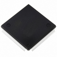
ST10F269Z2Q6 STMicroelectronics, ST10F269Z2Q6 Datasheet - Page 81

ST10F269Z2Q6
Manufacturer Part Number
ST10F269Z2Q6
Description
MCU 16BIT 256K FLASH 144PQFP
Manufacturer
STMicroelectronics
Series
ST10r
Specifications of ST10F269Z2Q6
Core Processor
ST10
Core Size
16-Bit
Speed
40MHz
Connectivity
CAN, EBI/EMI, SSC, UART/USART
Peripherals
POR, PWM, WDT
Number Of I /o
111
Program Memory Size
256KB (256K x 8)
Program Memory Type
FLASH
Ram Size
12K x 8
Voltage - Supply (vcc/vdd)
4.5 V ~ 5.5 V
Data Converters
A/D 16x10b
Oscillator Type
Internal
Operating Temperature
-40°C ~ 85°C
Package / Case
144-QFP
Controller Family/series
ST10
No. Of I/o's
111
Ram Memory Size
12KB
Cpu Speed
40MHz
No. Of Timers
5
Embedded Interface Type
CAN, SSC, USART
Rohs Compliant
Yes
Processor Series
ST10F26x
Core
ST10
Data Bus Width
16 bit
Data Ram Size
12 KB
Interface Type
CAN, SSC, USART
Maximum Clock Frequency
40 MHz
Number Of Programmable I/os
111
Number Of Timers
2 x 16 bit
Operating Supply Voltage
0.3 V to 4 V
Maximum Operating Temperature
+ 85 C
Mounting Style
SMD/SMT
Minimum Operating Temperature
- 40 C
On-chip Adc
16 bit x 10 bit
Lead Free Status / RoHS Status
Lead free / RoHS Compliant
Eeprom Size
-
Lead Free Status / Rohs Status
Details
Other names
497-4833
Available stocks
Company
Part Number
Manufacturer
Quantity
Price
Company:
Part Number:
ST10F269Z2Q6
Manufacturer:
ST
Quantity:
201
Company:
Part Number:
ST10F269Z2Q6
Manufacturer:
ST
Quantity:
745
Company:
Part Number:
ST10F269Z2Q6
Manufacturer:
STMicroelectronics
Quantity:
10 000
Part Number:
ST10F269Z2Q6
Manufacturer:
ST
Quantity:
20 000
The chip select lines of Port 6 have an internal
weak pull-up device. This device is switched on
during reset. This feature is implemented to drive
the chip select lines high during reset in order to
avoid multiple chip selection.
After reset the CS function must be used, if
selected so. In this case there is no possibility to
program any port latches before. Thus the
Figure 37 : Block Diagram of Port 6 Pins with an Alternate Output Function
Write ODP6.y
Read ODP6.y
Write DP6.y
Open Drain
Read DP6.y
Write DP6.y
Port Output
Read P6.y
Direction
Latch
Latch
Latch
MUX
Alternate
Data
Output
1
0
Alternate
Function
Enable
"1"
alternate function (CS) is selected automatically in
this case.
Note: The open drain output option can only be
"0"
1
0
1
0
MUX
MUX
selected via software earliest during the
initialization routine; at least signal CS0
will be in push/pull output driver mode
directly after reset.
1
0
MUX
MUX
Clock
Latch
Input
Output
Buffer
ST10F269-T3
y = (0...4, 6, 7)
P6.y
81/162


