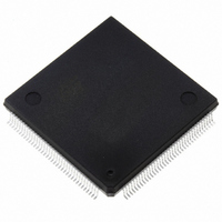
ST10F269Z2Q6 STMicroelectronics, ST10F269Z2Q6 Datasheet - Page 158

ST10F269Z2Q6
Manufacturer Part Number
ST10F269Z2Q6
Description
MCU 16BIT 256K FLASH 144PQFP
Manufacturer
STMicroelectronics
Series
ST10r
Specifications of ST10F269Z2Q6
Core Processor
ST10
Core Size
16-Bit
Speed
40MHz
Connectivity
CAN, EBI/EMI, SSC, UART/USART
Peripherals
POR, PWM, WDT
Number Of I /o
111
Program Memory Size
256KB (256K x 8)
Program Memory Type
FLASH
Ram Size
12K x 8
Voltage - Supply (vcc/vdd)
4.5 V ~ 5.5 V
Data Converters
A/D 16x10b
Oscillator Type
Internal
Operating Temperature
-40°C ~ 85°C
Package / Case
144-QFP
Controller Family/series
ST10
No. Of I/o's
111
Ram Memory Size
12KB
Cpu Speed
40MHz
No. Of Timers
5
Embedded Interface Type
CAN, SSC, USART
Rohs Compliant
Yes
Processor Series
ST10F26x
Core
ST10
Data Bus Width
16 bit
Data Ram Size
12 KB
Interface Type
CAN, SSC, USART
Maximum Clock Frequency
40 MHz
Number Of Programmable I/os
111
Number Of Timers
2 x 16 bit
Operating Supply Voltage
0.3 V to 4 V
Maximum Operating Temperature
+ 85 C
Mounting Style
SMD/SMT
Minimum Operating Temperature
- 40 C
On-chip Adc
16 bit x 10 bit
Lead Free Status / RoHS Status
Lead free / RoHS Compliant
Eeprom Size
-
Lead Free Status / Rohs Status
Details
Other names
497-4833
Available stocks
Company
Part Number
Manufacturer
Quantity
Price
Company:
Part Number:
ST10F269Z2Q6
Manufacturer:
ST
Quantity:
201
Company:
Part Number:
ST10F269Z2Q6
Manufacturer:
ST
Quantity:
745
Company:
Part Number:
ST10F269Z2Q6
Manufacturer:
STMicroelectronics
Quantity:
10 000
Part Number:
ST10F269Z2Q6
Manufacturer:
ST
Quantity:
20 000
ST10F269-T3
21.4.14.2 Slave mode
V
The formula for SSC Clock Cycle time is: t
Where <SSCBR> represents the content of the SSC Baud rate register, taken as unsigned 16-bit integer.
Figure 82 : SSC Slave Timing
Notes: 1. The phase and polarity of shift and latch edge of SCLK is programmable. This figure uses the leading clock edge as shift edge (drawn
158/162
t
t
318p
t
t
t
t
t
t
t
t
t
CC
317p
Symbol
310
311
312
313
314
315
316
317
318
= 5V ±10%, V
1
in bold), with latch on trailing edge (SSCPH = 0b), Idle clock line is low, leading clock edge is low-to-high transition (SSCPO = 0b).
2. The bit timing is repeated for all bits to be transmitted or received.
SCLK
MRST
MTSR
CC Write data valid after shift edge
CC Write data hold after shift edge
SR SSC clock cycle time
SR SSC clock high time
SR SSC clock low time
SR SSC clock rise time
SR SSC clock fall time
SR Read data setup time before latch edge,
SR Read data hold time after latch edge,
SR Read data setup time before latch edge,
SR Read data hold time after latch edge,
phase error detection on (SSCPEN = 1)
phase error detection on (SSCPEN = 1)
phase error detection off (SSCPEN = 0)
phase error detection off (SSCPEN = 0)
1)
SS
= 0V, CPU clock = 32MHz, T
Parameter
t
315
t
1st.In Bit
317
t
310
1st Out Bit
t
318
t
t
315
311
t
314
310
2nd Out Bit
t
= 4 TCL * (<SSCBR> + 1)
2nd.In Bit
Maximum Baud rate=6.25MBd
312
Minimum
109.375
78.125
A
41.25
(<SSCBR> = 0001h)
52.5
52.5
125
= -40 to +125°C, C
6
t
–
–
–
0
313
t
316
2)
Maximum
45.25
10
10
–
–
–
–
–
–
–
–
t
L
315
= 50pF
t
Last.In Bit
317
Last Out Bit
(<SSCBR>=0001h-FFFFh)
t
t
2TCL + 10
Minimum
310
310
4TCL +
6TCL +
t
15.625
15.625
8 TCL
318
Variable Baud rate
/2 - 10
/2 - 10
6
–
–
–
0
262144 TCL
2 TCL + 14
Maximum
10
10
–
–
–
–
–
–
–
Unit
ns
ns
ns
ns
ns
ns
ns
ns
ns
ns
ns


