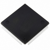
ST10F269Z2Q6 STMicroelectronics, ST10F269Z2Q6 Datasheet - Page 14

ST10F269Z2Q6
Manufacturer Part Number
ST10F269Z2Q6
Description
MCU 16BIT 256K FLASH 144PQFP
Manufacturer
STMicroelectronics
Series
ST10r
Specifications of ST10F269Z2Q6
Core Processor
ST10
Core Size
16-Bit
Speed
40MHz
Connectivity
CAN, EBI/EMI, SSC, UART/USART
Peripherals
POR, PWM, WDT
Number Of I /o
111
Program Memory Size
256KB (256K x 8)
Program Memory Type
FLASH
Ram Size
12K x 8
Voltage - Supply (vcc/vdd)
4.5 V ~ 5.5 V
Data Converters
A/D 16x10b
Oscillator Type
Internal
Operating Temperature
-40°C ~ 85°C
Package / Case
144-QFP
Controller Family/series
ST10
No. Of I/o's
111
Ram Memory Size
12KB
Cpu Speed
40MHz
No. Of Timers
5
Embedded Interface Type
CAN, SSC, USART
Rohs Compliant
Yes
Processor Series
ST10F26x
Core
ST10
Data Bus Width
16 bit
Data Ram Size
12 KB
Interface Type
CAN, SSC, USART
Maximum Clock Frequency
40 MHz
Number Of Programmable I/os
111
Number Of Timers
2 x 16 bit
Operating Supply Voltage
0.3 V to 4 V
Maximum Operating Temperature
+ 85 C
Mounting Style
SMD/SMT
Minimum Operating Temperature
- 40 C
On-chip Adc
16 bit x 10 bit
Lead Free Status / RoHS Status
Lead free / RoHS Compliant
Eeprom Size
-
Lead Free Status / Rohs Status
Details
Other names
497-4833
Available stocks
Company
Part Number
Manufacturer
Quantity
Price
Company:
Part Number:
ST10F269Z2Q6
Manufacturer:
ST
Quantity:
201
Company:
Part Number:
ST10F269Z2Q6
Manufacturer:
ST
Quantity:
745
Company:
Part Number:
ST10F269Z2Q6
Manufacturer:
STMicroelectronics
Quantity:
10 000
Part Number:
ST10F269Z2Q6
Manufacturer:
ST
Quantity:
20 000
ST10F269-T3
4 - MEMORY ORGANIZATION
The memory space of the ST10F269-T3 is
configured in a unified memory architecture. Code
memory, data memory, registers and I/O ports are
organized within the same linear address space of
16M Bytes. The entire memory space can be
accessed Byte wise or Word wise. Particular
portions of the on-chip memory have additionally
been made directly bit addressable.
Flash: 256K Bytes of on-chip Flash memory.
IRAM: 2K Bytes of on-chip internal RAM
(dual-port) is provided as a storage for data,
system stack, general purpose register banks and
code. A register bank is 16 Wordwide (R0 to R15)
and / or Bytewide (RL0, RH0, …, RL7, RH7)
general purpose registers.
XRAM: 10K Bytes of on-chip extension RAM
(single port XRAM) is provided as a storage for
data, user stack and code.
The XRAM is divided into 2 areas, the first 2K
Bytes named XRAM1 and the second 8K Bytes
named XRAM2, connected to the internal XBUS
and are accessed like an external memory in
16-bit demultiplexed bus-mode without wait state
or read/write delay (62.5ns access at 32MHz CPU
clock). Byte and Word accesses are allowed.
The
- 00’E7FFh if XPEN (bit 2 of SYSCON register),
and XRAM1EN (bit 2 of XPERCON register) are
set. If XRAM1EN or XPEN is cleared, then any
access in the address range 00’E000h - 00’E7FFh
will be directed to external memory interface,
using the BUSCONx register corresponding to
address matching ADDRSELx register
The
- 00’DFFFh if XPEN (bit 2 of SYSCON register),
and XRAM2 (bit 3 of XPERCON register are set).
If bit XRAM2EN or XPEN is cleared, then any
access
- 00’DFFFh will be directed to external memory
interface,
corresponding to address matching ADDRSELx
register.
As the XRAM appears like external memory, it
cannot be used as system stack or as register
banks. The XRAM is not provided for single bit
storage and therefore is not bit addressable.
14/162
XRAM2
XRAM1
in
using
the
address
address
address
the
range
range
BUSCONx
range
is
is
00’C000h
00’C000h
00’E000h
register
SFR/ESFR: 1024 Bytes (2 x 512 Bytes) of
address space is reserved for the special function
register areas. SFRs are Wordwide registers
which are used to control and to monitor the
function of the different on-chip units.
CAN1: Address range 00’EF00h - 00’EFFFh is
reserved for the CAN1 Module access. The CAN1
is enabled by setting XPEN bit 2 of the SYSCON
register and by setting CAN1EN bit 0 of the new
XPERCON register. Accesses to the CAN Module
use demultiplexed addresses and a 16-bit data
bus (Byte accesses are possible). Two wait states
give an access time of 125ns at 32MHz CPU
clock. No tri-state wait states are used.
CAN2: Address range 00’EE00h - 00’EEFFh is
reserved for the CAN2 Module access. The CAN2
is enabled by setting XPEN bit 2 of the SYSCON
register and by setting CAN2EN bit 1 of the new
XPERCON register. Accesses to the CAN Module
use demultiplexed addresses and a 16-bit data
bus (Byte accesses are possible). Two wait states
give an access time of 125ns at 32MHz CPU
clock. No tri-state wait states are used.
In order to meet the needs of designs where more
memory is required than is provided on chip, up to
16M Bytes of external RAM and/or ROM can be
connected to the microcontroller.
Note
Visibility of XBUS Peripherals
In order to keep the ST10F269-T3 compatible with
the ST10C167 and with the ST10F167, the XBUS
peripherals can be selected to be visible and / or
accessible on the external address / data bus.
CAN1EN and CAN2EN bits of XPERCON register
must be set. If these bits are cleared before the
global enabling with XPEN-bit in SYSCON
register, the corresponding address space, port
pins and interrupts are not occupied by the
peripheral, thus the peripheral is not visible and
not available. Refer to Chapter 20 - Special
Function Register Overview.
If one or the two CAN modules are used,
Port 4 cannot be programmed to output all
8 segment address lines. Thus, only 4
segment address lines can be used,
reducing the external memory space to 5M
Bytes (1M Byte per CS line).


