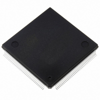
ST10F269Z2Q6 STMicroelectronics, ST10F269Z2Q6 Datasheet - Page 19

ST10F269Z2Q6
Manufacturer Part Number
ST10F269Z2Q6
Description
MCU 16BIT 256K FLASH 144PQFP
Manufacturer
STMicroelectronics
Series
ST10r
Specifications of ST10F269Z2Q6
Core Processor
ST10
Core Size
16-Bit
Speed
40MHz
Connectivity
CAN, EBI/EMI, SSC, UART/USART
Peripherals
POR, PWM, WDT
Number Of I /o
111
Program Memory Size
256KB (256K x 8)
Program Memory Type
FLASH
Ram Size
12K x 8
Voltage - Supply (vcc/vdd)
4.5 V ~ 5.5 V
Data Converters
A/D 16x10b
Oscillator Type
Internal
Operating Temperature
-40°C ~ 85°C
Package / Case
144-QFP
Controller Family/series
ST10
No. Of I/o's
111
Ram Memory Size
12KB
Cpu Speed
40MHz
No. Of Timers
5
Embedded Interface Type
CAN, SSC, USART
Rohs Compliant
Yes
Processor Series
ST10F26x
Core
ST10
Data Bus Width
16 bit
Data Ram Size
12 KB
Interface Type
CAN, SSC, USART
Maximum Clock Frequency
40 MHz
Number Of Programmable I/os
111
Number Of Timers
2 x 16 bit
Operating Supply Voltage
0.3 V to 4 V
Maximum Operating Temperature
+ 85 C
Mounting Style
SMD/SMT
Minimum Operating Temperature
- 40 C
On-chip Adc
16 bit x 10 bit
Lead Free Status / RoHS Status
Lead free / RoHS Compliant
Eeprom Size
-
Lead Free Status / Rohs Status
Details
Other names
497-4833
Available stocks
Company
Part Number
Manufacturer
Quantity
Price
Company:
Part Number:
ST10F269Z2Q6
Manufacturer:
ST
Quantity:
201
Company:
Part Number:
ST10F269Z2Q6
Manufacturer:
ST
Quantity:
745
Company:
Part Number:
ST10F269Z2Q6
Manufacturer:
STMicroelectronics
Quantity:
10 000
Part Number:
ST10F269Z2Q6
Manufacturer:
ST
Quantity:
20 000
be temporarily unlocked for update (write)
operations.
With the two possibilities for write protection -
whole memory or block specific - a flexible
installation of write protection is supported to
protect the Flash memory or parts of it from
unauthorized programming or erase accesses
and to provide virus-proof protection for all system
code blocks. All write protection also is enabled
during boot operation.
Power Supply, Reset
The Flash module uses a single power supply for
both read and write functions. Internally generated
and regulated voltages are provided for the
program and erase operations from 5V supply.
Once a program or erase cycle has been
completed, the device resets to the standard read
mode. At power-on, the Flash memory has a setup
phase of some microseconds (dependent on the
power supply ramp-up). During this phase, Flash
can not be read. Thus, if EA pin is high (execution
will start from Flash memory), the CPU will remains
in reset state until the Flash can be accessed.
5.3 - Architectural Description
The Flash module distinguishes two basic
operating modes, the standard read mode and the
command mode. The initial state after power-on
and after reset is the standard read mode.
5.3.1 - Read Mode
The Flash module enters the standard operating
mode, the read mode:
– After Reset command
– After every completed erase operation
– After every completed programming operation
– After
– Few microseconds after a CPU-reset has
– After incorrect address and data values of
– After incorrect write access to a read protected
The read mode remains active until the last
command of a command sequence is decoded
which starts directly a Flash array operation, such
as:
– erase one or several blocks
– program a word into Flash array
– protected / temporary unprotected a block.
execution
started
command sequences or writing them in an
improper sequence
Flash memory
every
other
completed
command
In the standard read mode read accesses are
directly controlled by the Flash memory array,
delivering a 32-bit double Word from the
addressed position. Read accesses are always
aligned to double Word boundaries. Thus, both
low order address bit A1 and A0 are not used in
the Flash array for read accesses. The high order
address bit A17/A16 define the physical 64K Byte
segment being accessed within the Flash array.
5.3.2 - Command Mode
Every operation besides standard read operations
is initiated by commands written to the Flash
command register. The addresses used for
command cycles define in conjunction with the
actual state the specific step within command
sequences. With the last command of a command
sequence, the Erase-Program Controller (EPC)
starts the execution of the command. The EPC
status is indicated during command execution by:
– The Status Register,
– The Ready/Busy signal.
5.3.3 - Ready/Busy Signal
The Ready/Busy (R/B) signal is connected to the
XPER2 interrupt node (XP2IC). When R/B is high,
the Flash is busy with a Program or Erase
operation and will not accept any additional
program or erase instruction. When R/B is Low,
the Flash is ready for any Read/Write or Erase
operation. The R/B will also be low when the
memory is put in Erase Suspend mode.
This signal can be polled by reading XP2IC
register, or can be used to trigger an interrupt
when the Flash goes from Busy to Ready.
5.3.4 - Flash Status Register
The Flash Status register is used to flag the status
of the Flash memory and the result of an
operation. This register can be accessed by Read
cycles during the program-Erase Controller
operations. The program or erase operation can
be controlled by data polling on bit FSB.7 of
Status Register, detection of Toggle on FSB.6 and
FSB.2, or Error on FSB.5 and Erase Time-out on
FSB.3 bit. Any read attempt in Flash during EPC
operation will automatically output these five bits.
The EPC sets bit FSB.2, FSB.3, FSB.5, FSB.6
and FSB.7. Other bits are reserved for future use
and should be masked.
ST10F269-T3
19/162


