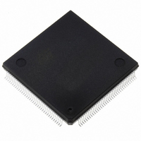
ST10F269Z2Q6 STMicroelectronics, ST10F269Z2Q6 Datasheet - Page 24

ST10F269Z2Q6
Manufacturer Part Number
ST10F269Z2Q6
Description
MCU 16BIT 256K FLASH 144PQFP
Manufacturer
STMicroelectronics
Series
ST10r
Specifications of ST10F269Z2Q6
Core Processor
ST10
Core Size
16-Bit
Speed
40MHz
Connectivity
CAN, EBI/EMI, SSC, UART/USART
Peripherals
POR, PWM, WDT
Number Of I /o
111
Program Memory Size
256KB (256K x 8)
Program Memory Type
FLASH
Ram Size
12K x 8
Voltage - Supply (vcc/vdd)
4.5 V ~ 5.5 V
Data Converters
A/D 16x10b
Oscillator Type
Internal
Operating Temperature
-40°C ~ 85°C
Package / Case
144-QFP
Controller Family/series
ST10
No. Of I/o's
111
Ram Memory Size
12KB
Cpu Speed
40MHz
No. Of Timers
5
Embedded Interface Type
CAN, SSC, USART
Rohs Compliant
Yes
Processor Series
ST10F26x
Core
ST10
Data Bus Width
16 bit
Data Ram Size
12 KB
Interface Type
CAN, SSC, USART
Maximum Clock Frequency
40 MHz
Number Of Programmable I/os
111
Number Of Timers
2 x 16 bit
Operating Supply Voltage
0.3 V to 4 V
Maximum Operating Temperature
+ 85 C
Mounting Style
SMD/SMT
Minimum Operating Temperature
- 40 C
On-chip Adc
16 bit x 10 bit
Lead Free Status / RoHS Status
Lead free / RoHS Compliant
Eeprom Size
-
Lead Free Status / Rohs Status
Details
Other names
497-4833
Available stocks
Company
Part Number
Manufacturer
Quantity
Price
Company:
Part Number:
ST10F269Z2Q6
Manufacturer:
ST
Quantity:
201
Company:
Part Number:
ST10F269Z2Q6
Manufacturer:
ST
Quantity:
745
Company:
Part Number:
ST10F269Z2Q6
Manufacturer:
STMicroelectronics
Quantity:
10 000
Part Number:
ST10F269Z2Q6
Manufacturer:
ST
Quantity:
20 000
ST10F269-T3
Table 3 : Instructions
Notes 1. Address bit A14, A15 and above are don’t care for coded address inputs.
24/162
Read/Reset
Read/Reset
Program Word
Block Erase
Chip Erase
Erase Suspend
Erase Resume
Set Block/Code
Protection
Read
Protection
Status
Block
Temporary
Unprotection
Code
Temporary
Unprotection
Code
Temporary
Protection
Instruction
2. X = Don’t Care.
3. WA = Write Address: address of memory location to be programmed.
4. WD = Write Data: 16-bit data to be programmed
5. Optional, additional blocks addresses must be entered within a time-out delay (96 µs) after last write entry, time-out status can be
verified through FSB.3 value. When full command is entered, read Data Polling or Toggle bit until Erase is completed or suspended.
6. Read Data Polling or Toggle bit until Erase completes.
7. WPR = Write protection register. To protect code, bit 15 of WPR must be ‘0’. To protect block N (N=0,1,...), bit N of WPR must be
‘0’. Bit that are already at ‘0’ in protection register must also be ‘0’ in WPR, else a writing error will occurs (it is not possible to write a
‘1’ in a bit already programmed at ‘0’).
8. MEM = any address inside the Flash memory space. Absolute addressing mode must be used (MOV MEM, Rn), and instruction
must be executed from Flash memory space.
9. Odd word address = 4n-2 where n = 0, 1, 2, 3..., ex. 0002h, 0006h...
CTU
Mne Cycle
BTU
CTP
PW
RD
RD
BE
CE
ES
ER
SP
RP
1+
3+
4
6
6
1
1
4
4
4
1
1
Addr.
Addr.
Addr.
Addr.
Addr.
Addr.
Addr.
Addr.
Addr.
Addr.
Addr.
Addr.
Data
Data
Data
Data
Data
Data
Data
Data
Data
Data
Data
Data
1
1
1
1
1
1
1
1
1
1
1
1
x2A54h
x2A54h
x2A54h
x1554h
x1554h
x1554h
x1554h
MEM
FFFFh
MEM
FFFBh
xxA8h
xxA8h
xxA8h
xxA8h
xxB0h
xxA8h
xxA8h
xxA8h
Cycle
xxF0h
xx30h
X
1
X
X
st
2
2
2
8
8
Read Memory Array until a new write cycle is initiated
Read until Toggle stops, then read or program all data needed
from block(s) not being erased then Resume Erase.
Read Data Polling or Toggle bit until Erase completes or Erase is
suspended another time.
Write cycles must be executed from Flash.
Write cycles must be executed from Flash.
x2AA8h
x2AA8h
x2AA8h
x2AA8h
x15A8h
x15A8h
x15A8h
Cycle
xx54h
xx54h
xx54h
xx54h
xx54h
xx54h
xx54h
2
nd
3
x1554h
x1554h
x1554h
x2A54h
x2A54h
x2A54h
rd
xxxxxh
xxC0h
xxC1h
xxF0h
xxA0h
xx80h
xx80h
xx90h
Cycle
Read Memory Array until a new write
cycle is initiated
Read PR
4
address
address
Any odd
Any odd
x1554h
x1554h
th
WPR
xxA8h
xxA8h
xxF0h
WD
WA
word
word
Cycle
X
2
3
4
7
9
9
Read Protection Register
until a new write cycle is
initiated.
x2AA8h
x2AA8h
Cycle
Read Data Polling or Tog-
gle bit until Program com-
xx54h
xx54h
5
th
pletes.
x1554h
xx30h
xx10h
Cycle
6
BA
th
Note
Cycle
xx30h
BA’
7
th
5
6


