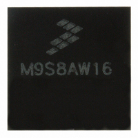
MC9S08AW16MFGE Freescale Semiconductor, MC9S08AW16MFGE Datasheet - Page 191

MC9S08AW16MFGE
Manufacturer Part Number
MC9S08AW16MFGE
Description
IC MCU 8BIT 16K FLASH 44-LQFP
Manufacturer
Freescale Semiconductor
Series
HCS08r
Datasheet
1.MC9S08AW32CFDE.pdf
(324 pages)
Specifications of MC9S08AW16MFGE
Core Processor
HCS08
Core Size
8-Bit
Speed
40MHz
Connectivity
I²C, SCI, SPI
Peripherals
LVD, POR, PWM, WDT
Number Of I /o
34
Program Memory Size
16KB (16K x 8)
Program Memory Type
FLASH
Ram Size
1K x 8
Voltage - Supply (vcc/vdd)
2.7 V ~ 5.5 V
Data Converters
A/D 8x10b
Oscillator Type
Internal
Operating Temperature
-40°C ~ 125°C
Package / Case
44-LQFP
Lead Free Status / RoHS Status
Lead free / RoHS Compliant
Eeprom Size
-
Available stocks
Company
Part Number
Manufacturer
Quantity
Price
Company:
Part Number:
MC9S08AW16MFGE
Manufacturer:
Freescale Semiconductor
Quantity:
10 000
Part Number:
MC9S08AW16MFGE
Manufacturer:
FREESCALE
Quantity:
20 000
- Current page: 191 of 324
- Download datasheet (4Mb)
11.2.5
This register has one read-only status flag. Writes have no effect.
11.2.6
Freescale Semiconductor
Reset
Reset
BRK13
Field
Field
RAF
R8
T8
2
0
7
6
W
W
R
R
SCI Status Register 2 (SCIxS2)
SCI Control Register 3 (SCIxC3)
Break Character Length — BRK13 is used to select a longer break character length. Detection of a framing
error is not affected by the state of this bit.
0 Break character is 10 bit times (11 if M = 1)
1 Break character is 13 bit times (14 if M = 1)
Receiver Active Flag — RAF is set when the SCI receiver detects the beginning of a valid start bit, and RAF is
cleared automatically when the receiver detects an idle line. This status flag can be used to check whether an
SCI character is being received before instructing the MCU to go to stop mode.
0 SCI receiver idle waiting for a start bit.
1 SCI receiver active (RxD input not idle).
Ninth Data Bit for Receiver — When the SCI is configured for 9-bit data (M = 1), R8 can be thought of as a
ninth receive data bit to the left of the MSB of the buffered data in the SCIxD register. When reading 9-bit data,
both R8 and SCIxD must be read to complete the automatic RDRF clearing sequence.
Ninth Data Bit for Transmitter — When the SCI is configured for 9-bit data (M = 1), T8 may be thought of as a
ninth transmit data bit to the left of the MSB of the data in the SCIxD register. When writing 9-bit data, the entire
9-bit value is transferred to the SCI shift register after SCIxD is written so T8 should be written (if it needs to
change from its previous value) before SCIxD is written. If T8 does not need to change in the new value (such
as when it is used to generate mark or space parity), it need not be written each time SCIxD is written.
R8
0
0
0
7
7
= Unimplemented or Reserved
= Unimplemented or Reserved
T8
0
0
0
6
6
Table 11-7. SCIxC3 Register Field Descriptions
Table 11-6. SCIxS2 Register Field Descriptions
Figure 11-10. SCI Control Register 3 (SCIxC3)
Figure 11-9. SCI Status Register 2 (SCIxS2)
TXDIR
0
0
0
5
5
MC9S08AW60 Data Sheet, Rev 2
TXINV
0
0
0
4
4
Description
Description
ORIE
Chapter 11 Serial Communications Interface (S08SCIV2)
3
0
0
3
0
BRK13
NEIE
0
0
2
2
FEIE
0
0
0
1
1
PEIE
RAF
0
0
0
0
191
Related parts for MC9S08AW16MFGE
Image
Part Number
Description
Manufacturer
Datasheet
Request
R
Part Number:
Description:
Manufacturer:
Freescale Semiconductor, Inc
Datasheet:
Part Number:
Description:
Manufacturer:
Freescale Semiconductor, Inc
Datasheet:
Part Number:
Description:
Manufacturer:
Freescale Semiconductor, Inc
Datasheet:
Part Number:
Description:
Manufacturer:
Freescale Semiconductor, Inc
Datasheet:
Part Number:
Description:
Manufacturer:
Freescale Semiconductor, Inc
Datasheet:
Part Number:
Description:
Manufacturer:
Freescale Semiconductor, Inc
Datasheet:
Part Number:
Description:
Manufacturer:
Freescale Semiconductor, Inc
Datasheet:
Part Number:
Description:
Manufacturer:
Freescale Semiconductor, Inc
Datasheet:
Part Number:
Description:
Manufacturer:
Freescale Semiconductor, Inc
Datasheet:
Part Number:
Description:
Manufacturer:
Freescale Semiconductor, Inc
Datasheet:
Part Number:
Description:
Manufacturer:
Freescale Semiconductor, Inc
Datasheet:
Part Number:
Description:
Manufacturer:
Freescale Semiconductor, Inc
Datasheet:
Part Number:
Description:
Manufacturer:
Freescale Semiconductor, Inc
Datasheet:
Part Number:
Description:
Manufacturer:
Freescale Semiconductor, Inc
Datasheet:
Part Number:
Description:
Manufacturer:
Freescale Semiconductor, Inc
Datasheet:


