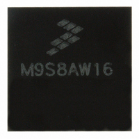
MC9S08AW16MFGE Freescale Semiconductor, MC9S08AW16MFGE Datasheet - Page 72

MC9S08AW16MFGE
Manufacturer Part Number
MC9S08AW16MFGE
Description
IC MCU 8BIT 16K FLASH 44-LQFP
Manufacturer
Freescale Semiconductor
Series
HCS08r
Datasheet
1.MC9S08AW32CFDE.pdf
(324 pages)
Specifications of MC9S08AW16MFGE
Core Processor
HCS08
Core Size
8-Bit
Speed
40MHz
Connectivity
I²C, SCI, SPI
Peripherals
LVD, POR, PWM, WDT
Number Of I /o
34
Program Memory Size
16KB (16K x 8)
Program Memory Type
FLASH
Ram Size
1K x 8
Voltage - Supply (vcc/vdd)
2.7 V ~ 5.5 V
Data Converters
A/D 8x10b
Oscillator Type
Internal
Operating Temperature
-40°C ~ 125°C
Package / Case
44-LQFP
Lead Free Status / RoHS Status
Lead free / RoHS Compliant
Eeprom Size
-
Available stocks
Company
Part Number
Manufacturer
Quantity
Price
Company:
Part Number:
MC9S08AW16MFGE
Manufacturer:
Freescale Semiconductor
Quantity:
10 000
Part Number:
MC9S08AW16MFGE
Manufacturer:
FREESCALE
Quantity:
20 000
- Current page: 72 of 324
- Download datasheet (4Mb)
Chapter 5 Resets, Interrupts, and System Configuration
Either RTI clock source can be used when the MCU is in run, wait or stop3 mode. When using the external
oscillator in stop3, it must be enabled in stop (OSCSTEN = 1) and configured for low bandwidth operation
(RANGE = 0). Only the internal 1-kHz clock source can be selected to wake the MCU from stop2 mode.
The SRTISC register includes a read-only status flag, a write-only acknowledge bit, and a 3-bit control
value (RTIS2:RTIS1:RTIS0) used to disable the clock source to the real-time interrupt or select one of
seven wakeup periods. The RTI has a local interrupt enable, RTIE, to allow masking of the real-time
interrupt. The RTI can be disabled by writing each bit of RTIS to zeroes, and no interrupts will be
generated. See
detailed information about this register.
5.8
The PTC2 pin is shared with the MCLK clock output. Setting the pin enable bit, MPE, causes the PTC2
pin to output a divided version of the internal MCU bus clock. The divide ratio is determined by the
MCSEL bits. When MPE is set, the PTC2 pin is forced to operate as an output pin regardless of the state
of the port data direction control bit for the pin. If the MCSEL bits are all 0s, the pin is driven low. The
slew rate and drive strength for the pin are controlled by PTCSE2 and PTCDS2, respectively. The
maximum clock output frequency is limited if slew rate control is enabled, see
Characteristics and Timing
5.9
One 8-bit register in the direct page register space and eight 8-bit registers in the high-page register space
are related to reset and interrupt systems.
Refer to the direct-page register summary in
address assignments for all registers. This section refers to registers and control bits only by their names.
A Freescale-provided equate or header file is used to translate these names into the appropriate absolute
addresses.
Some control bits in the SOPT and SPMSC2 registers are related to modes of operation. Although brief
descriptions of these bits are provided here, the related functions are discussed in greater detail in
Chapter 3, “Modes of
72
MCLK Output
Reset, Interrupt, and System Control Registers and Control Bits
Section 5.9.7, “System Real-Time Interrupt Status and Control Register
Operation.”
Specifications,” for pin rise and fall times with slew rate enabled.
MC9S08AW60 Data Sheet, Rev 2
Chapter 4,
“Memory,” of this data sheet for the absolute
Appendix A, “Electrical
Freescale Semiconductor
(SRTISC),” for
Related parts for MC9S08AW16MFGE
Image
Part Number
Description
Manufacturer
Datasheet
Request
R
Part Number:
Description:
Manufacturer:
Freescale Semiconductor, Inc
Datasheet:
Part Number:
Description:
Manufacturer:
Freescale Semiconductor, Inc
Datasheet:
Part Number:
Description:
Manufacturer:
Freescale Semiconductor, Inc
Datasheet:
Part Number:
Description:
Manufacturer:
Freescale Semiconductor, Inc
Datasheet:
Part Number:
Description:
Manufacturer:
Freescale Semiconductor, Inc
Datasheet:
Part Number:
Description:
Manufacturer:
Freescale Semiconductor, Inc
Datasheet:
Part Number:
Description:
Manufacturer:
Freescale Semiconductor, Inc
Datasheet:
Part Number:
Description:
Manufacturer:
Freescale Semiconductor, Inc
Datasheet:
Part Number:
Description:
Manufacturer:
Freescale Semiconductor, Inc
Datasheet:
Part Number:
Description:
Manufacturer:
Freescale Semiconductor, Inc
Datasheet:
Part Number:
Description:
Manufacturer:
Freescale Semiconductor, Inc
Datasheet:
Part Number:
Description:
Manufacturer:
Freescale Semiconductor, Inc
Datasheet:
Part Number:
Description:
Manufacturer:
Freescale Semiconductor, Inc
Datasheet:
Part Number:
Description:
Manufacturer:
Freescale Semiconductor, Inc
Datasheet:
Part Number:
Description:
Manufacturer:
Freescale Semiconductor, Inc
Datasheet:


