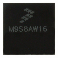
MC9S08AW16MFGE Freescale Semiconductor, MC9S08AW16MFGE Datasheet - Page 83

MC9S08AW16MFGE
Manufacturer Part Number
MC9S08AW16MFGE
Description
IC MCU 8BIT 16K FLASH 44-LQFP
Manufacturer
Freescale Semiconductor
Series
HCS08r
Datasheet
1.MC9S08AW32CFDE.pdf
(324 pages)
Specifications of MC9S08AW16MFGE
Core Processor
HCS08
Core Size
8-Bit
Speed
40MHz
Connectivity
I²C, SCI, SPI
Peripherals
LVD, POR, PWM, WDT
Number Of I /o
34
Program Memory Size
16KB (16K x 8)
Program Memory Type
FLASH
Ram Size
1K x 8
Voltage - Supply (vcc/vdd)
2.7 V ~ 5.5 V
Data Converters
A/D 8x10b
Oscillator Type
Internal
Operating Temperature
-40°C ~ 125°C
Package / Case
44-LQFP
Lead Free Status / RoHS Status
Lead free / RoHS Compliant
Eeprom Size
-
Available stocks
Company
Part Number
Manufacturer
Quantity
Price
Company:
Part Number:
MC9S08AW16MFGE
Manufacturer:
Freescale Semiconductor
Quantity:
10 000
Part Number:
MC9S08AW16MFGE
Manufacturer:
FREESCALE
Quantity:
20 000
- Current page: 83 of 324
- Download datasheet (4Mb)
Port B pins are general-purpose I/O pins. Parallel I/O function is controlled by the port B data (PTBD) and
data direction (PTBDD) registers which are located in page zero register space. The pin control registers,
pullup enable (PTBPE), slew rate control (PTBSE), and drive strength select (PTBDS) are located in the
high page registers. Refer to
general-purpose I/O control and
Port B general-purpose I/O are shared with the ADC. Any pin enabled as an ADC input will have the
general-purpose I/O function disabled. Refer to
(S08ADC10V1)” for more information about using port B as analog inputs.
6.3.3
Port C pins are general-purpose I/O pins. Parallel I/O function is controlled by the port C data (PTCD) and
data direction (PTCDD) registers which are located in page zero register space. The pin control registers,
pullup enable (PTCPE), slew rate control (PTCSE), and drive strength select (PTCDS) are located in the
high page registers. Refer to
general-purpose I/O control and
Port C general-purpose I/O is shared with SCI2, IIC, and MCLK. When any of these shared functions is
enabled, the direction, input or output, is controlled by the shared function and not by the data direction
register of the parallel I/O port. Also, for pins which are configured as outputs by the shared function, the
output data is controlled by the shared function and not by the port data register.
Refer to
port C pins as SCI pins.
Refer to
as IIC pins.
Refer to
PTC2 as the MCLK pin.
6.3.4
Port D pins are general-purpose I/O pins. Parallel I/O function is controlled by the port D data (PTDD) and
data direction (PTDDD) registers which are located in page zero register space. The pin control registers,
Freescale Semiconductor
Port C
Port D
Chapter 11, “Serial Communications Interface
Chapter 13, “Inter-Integrated Circuit
Chapter 5, “Resets, Interrupts, and System
Port C
Port D
MCU Pin:
MCU Pin:
AD1P15/
KBI1P7
PTD7/
Section 6.4, “Parallel I/O
Section 6.4, “Parallel I/O
Bit 7
Bit 7
Section 6.5, “Pin
Section 6.5, “Pin
TPM1CLK
AD1P14/
PTC6
PTD6/
Figure 6-3. Port C Pin Names
Figure 6-4. Port D Pin Names
MC9S08AW60 Data Sheet, Rev 2
6
6
(S08IICV1)” for more information about using port C pins
AD1P13/
PTC5/
RxD2
PTD5/
Chapter 14, “Analog-to-Digital Converter
5
5
Control” for more information about pin control.
Control” for more information about pin control.
Configuration” for more information about using
TPM2CLK
Control” for more information about
Control” for more information about
AD1P12/
PTC4
(S08SCIV2)” for more information about using
PTD4/
3
4
AD1P11/
KBI1P6
PTC3/
PTD3/
TxD2
3
3
AD1P10/
KBI1P5
PTC2/
MCLK
PTD2/
2
2
Chapter 6 Parallel Input/Output
PTC1/
AD1P9
SDA1
PTD1/
1
1
PTC0/
AD1P8
SCL1
PTD0/
Bit 0
Bit 0
83
Related parts for MC9S08AW16MFGE
Image
Part Number
Description
Manufacturer
Datasheet
Request
R
Part Number:
Description:
Manufacturer:
Freescale Semiconductor, Inc
Datasheet:
Part Number:
Description:
Manufacturer:
Freescale Semiconductor, Inc
Datasheet:
Part Number:
Description:
Manufacturer:
Freescale Semiconductor, Inc
Datasheet:
Part Number:
Description:
Manufacturer:
Freescale Semiconductor, Inc
Datasheet:
Part Number:
Description:
Manufacturer:
Freescale Semiconductor, Inc
Datasheet:
Part Number:
Description:
Manufacturer:
Freescale Semiconductor, Inc
Datasheet:
Part Number:
Description:
Manufacturer:
Freescale Semiconductor, Inc
Datasheet:
Part Number:
Description:
Manufacturer:
Freescale Semiconductor, Inc
Datasheet:
Part Number:
Description:
Manufacturer:
Freescale Semiconductor, Inc
Datasheet:
Part Number:
Description:
Manufacturer:
Freescale Semiconductor, Inc
Datasheet:
Part Number:
Description:
Manufacturer:
Freescale Semiconductor, Inc
Datasheet:
Part Number:
Description:
Manufacturer:
Freescale Semiconductor, Inc
Datasheet:
Part Number:
Description:
Manufacturer:
Freescale Semiconductor, Inc
Datasheet:
Part Number:
Description:
Manufacturer:
Freescale Semiconductor, Inc
Datasheet:
Part Number:
Description:
Manufacturer:
Freescale Semiconductor, Inc
Datasheet:


