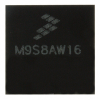
MC9S08AW16MFGE Freescale Semiconductor, MC9S08AW16MFGE Datasheet - Page 36

MC9S08AW16MFGE
Manufacturer Part Number
MC9S08AW16MFGE
Description
IC MCU 8BIT 16K FLASH 44-LQFP
Manufacturer
Freescale Semiconductor
Series
HCS08r
Datasheet
1.MC9S08AW32CFDE.pdf
(324 pages)
Specifications of MC9S08AW16MFGE
Core Processor
HCS08
Core Size
8-Bit
Speed
40MHz
Connectivity
I²C, SCI, SPI
Peripherals
LVD, POR, PWM, WDT
Number Of I /o
34
Program Memory Size
16KB (16K x 8)
Program Memory Type
FLASH
Ram Size
1K x 8
Voltage - Supply (vcc/vdd)
2.7 V ~ 5.5 V
Data Converters
A/D 8x10b
Oscillator Type
Internal
Operating Temperature
-40°C ~ 125°C
Package / Case
44-LQFP
Lead Free Status / RoHS Status
Lead free / RoHS Compliant
Eeprom Size
-
Available stocks
Company
Part Number
Manufacturer
Quantity
Price
Company:
Part Number:
MC9S08AW16MFGE
Manufacturer:
Freescale Semiconductor
Quantity:
10 000
Part Number:
MC9S08AW16MFGE
Manufacturer:
FREESCALE
Quantity:
20 000
- Current page: 36 of 324
- Download datasheet (4Mb)
Chapter 3 Modes of Operation
After waking up from stop2, the PPDF bit in SPMSC2 is set. This flag may be used to direct user code to
go to a stop2 recovery routine. PPDF remains set and the I/O pin states remain latched until a logic 1 is
written to PPDACK in SPMSC2.
To maintain I/O state for pins that were configured as general-purpose I/O, the user must restore the
contents of the I/O port registers, which have been saved in RAM, to the port registers before writing to
the PPDACK bit. If the port registers are not restored from RAM before writing to PPDACK, then the
register bits will assume their reset states when the I/O pin latches are opened and the I/O pins will switch
to their reset states.
For pins that were configured as peripheral I/O, the user must reconfigure the peripheral module that
interfaces to the pin before writing to the PPDACK bit. If the peripheral module is not enabled before
writing to PPDACK, the pins will be controlled by their associated port control registers when the I/O
latches are opened.
3.6.2
Stop3 mode is entered by executing a STOP instruction under the conditions as shown in
states of all of the internal registers and logic, RAM contents, and I/O pin states are maintained.
Stop3 can be exited by asserting RESET, or by an interrupt from one of the following sources: the real-time
interrupt (RTI), LVD, ADC, IRQ, or the KBI.
If stop3 is exited by means of the RESET pin, then the MCU is reset and operation will resume after taking
the reset vector. Exit by means of one of the internal interrupt sources results in the MCU taking the
appropriate interrupt vector.
3.6.3
Entry into the active background mode from run mode is enabled if the ENBDM bit in BDCSCR is set.
This register is described in
the CPU executes a STOP instruction, the system clocks to the background debug logic remain active when
the MCU enters stop mode so background debug communication is still possible. In addition, the voltage
regulator does not enter its low-power standby state but maintains full internal regulation. If the user
attempts to enter stop2 with ENBDM set, the MCU will instead enter stop3.
Most background commands are not available in stop mode. The memory-access-with-status commands
do not allow memory access, but they report an error indicating that the MCU is in either stop or wait
mode. The BACKGROUND command can be used to wake the MCU from stop and enter active
background mode if the ENBDM bit is set. After entering background debug mode, all background
commands are available.
background debug mode is enabled.
36
Stop3 Mode
Active BDM Enabled in Stop Mode
Table 3-2
Chapter 15, “Development
summarizes the behavior of the MCU in stop when entry into the
MC9S08AW60 Data Sheet, Rev 2
Support” of this data sheet. If ENBDM is set when
Freescale Semiconductor
Table
3-1. The
Related parts for MC9S08AW16MFGE
Image
Part Number
Description
Manufacturer
Datasheet
Request
R
Part Number:
Description:
Manufacturer:
Freescale Semiconductor, Inc
Datasheet:
Part Number:
Description:
Manufacturer:
Freescale Semiconductor, Inc
Datasheet:
Part Number:
Description:
Manufacturer:
Freescale Semiconductor, Inc
Datasheet:
Part Number:
Description:
Manufacturer:
Freescale Semiconductor, Inc
Datasheet:
Part Number:
Description:
Manufacturer:
Freescale Semiconductor, Inc
Datasheet:
Part Number:
Description:
Manufacturer:
Freescale Semiconductor, Inc
Datasheet:
Part Number:
Description:
Manufacturer:
Freescale Semiconductor, Inc
Datasheet:
Part Number:
Description:
Manufacturer:
Freescale Semiconductor, Inc
Datasheet:
Part Number:
Description:
Manufacturer:
Freescale Semiconductor, Inc
Datasheet:
Part Number:
Description:
Manufacturer:
Freescale Semiconductor, Inc
Datasheet:
Part Number:
Description:
Manufacturer:
Freescale Semiconductor, Inc
Datasheet:
Part Number:
Description:
Manufacturer:
Freescale Semiconductor, Inc
Datasheet:
Part Number:
Description:
Manufacturer:
Freescale Semiconductor, Inc
Datasheet:
Part Number:
Description:
Manufacturer:
Freescale Semiconductor, Inc
Datasheet:
Part Number:
Description:
Manufacturer:
Freescale Semiconductor, Inc
Datasheet:


