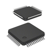
DF71241D50FPV Renesas Electronics America, DF71241D50FPV Datasheet - Page 779

DF71241D50FPV
Manufacturer Part Number
DF71241D50FPV
Description
MCU RISC FLASH 5V 32K 48-LQFP
Manufacturer
Renesas Electronics America
Series
SuperH® SH Tinyr
Datasheet
1.DF71243N50FPV.pdf
(794 pages)
Specifications of DF71241D50FPV
Core Processor
SH-2
Core Size
32-Bit
Speed
50MHz
Connectivity
SCI
Peripherals
POR, PWM, WDT
Number Of I /o
23
Program Memory Size
32KB (32K x 8)
Program Memory Type
FLASH
Ram Size
8K x 8
Voltage - Supply (vcc/vdd)
4 V ~ 5.5 V
Data Converters
A/D 8x10b
Oscillator Type
External
Operating Temperature
-40°C ~ 85°C
Package / Case
48-LQFP
Lead Free Status / RoHS Status
Lead free / RoHS Compliant
Eeprom Size
-
Available stocks
Company
Part Number
Manufacturer
Quantity
Price
Company:
Part Number:
DF71241D50FPV
Manufacturer:
Renesas Electronics America
Quantity:
10 000
- Current page: 779 of 794
- Download datasheet (5Mb)
Item
16.1 Port A
Figure 16.1 Port A (SH7125)
Figure 16.2 Port A (SH7124)
16.5 Usage Notes
16.5.1 Handling of Unused Pins
17. Flash Memory (ROM)
Page Revision (See Manual for Details)
554
554
577
579
Figure amended
This LSI has 128-Kbyte, 64-Kbyte, 32-Kbyte, or 16-
Kbyte on-chip flash memory. The flash memory has the
following features.
Figure amended
Newly added
Description amended
Port A
Port A
Note: * The TDO, TDI, TCK, TMS, and TRST pins are not supported on the 32 Kbyte (SH71251A and SH71241A) and
Note: * The TDO, TDI, TCK, TMS, and TRST pins are not supported on the 32 Kbyte (SH71251A and SH71241A) and
16 Kbyte (SH71250A and SH71240A) versions.
16 Kbyte (SH71250A and SH71240A) versions.
PA9 (I/O)/ TCLKD (input)/ TXD2 (output)/ TDO* (output)/ POE8 (input)
PA8 (I/O)/ TCLKC (input)/ RXD2 (input)/ TDI* (input)
PA7 (I/O)/ TCLKB (input)/ SCK2 (I/O)/ TCK* (input)
PA6 (I/O)/ TCLKA (input)
PA4 (I/O)/I RQ2 (input)/ TXD1 (output)/ TMS* (input)
PA3 (I/O)/ IRQ1 (input)/ RXD1 (input)/ TRST* (input)
PA1 (I/O)/ POE1 (input)/ TXD0 (output)
PA0 (I/O)/ POE0 (input)/ RXD0 (input)
PA15 (I/O)/ TXD1 (output)
PA14 (I/O)/ RXD1 (input)
PA13 (I/O)/ SCK1 (I/O)
PA12 (I/O)/ SCK0 (I/O)
PA11 (I/O)/ TXD0 (output)/ ADTRG (input)
PA10 (I/O)/ RXD0 (input)
PA9 (I/O)/ TCLKD (input)/ TXD2 (output)/ TDO* (output)/ POE8 (input)
PA8 (I/O)/ TCLKC (input)/ RXD2 (input)/ TDI* (input)
PA7 (I/O)/ TCLKB (input)/ SCK2 (I/O)/ TCK* (input)
PA6 (I/O)/ TCLKA (input)
PA5 (I/O)/ IRQ3 (input)/ SCK1 (I/O)
PA4 (I/O)/I RQ2 (input)/ TXD1 (output)/ TMS* (input)
PA3 (I/O)/ IRQ1 (input)/ RXD1 (input)/ TRST* (input)
PA2 (I/O)/ IRQ0 (input)/ SCK0 (I/O)
PA1 (I/O)/ POE1 (input)/ TXD0 (output)
PA0 (I/O)/ POE0 (input)/ RXD0 (input)
Rev. 5.00 Mar. 06, 2009 Page 759 of 770
REJ09B0243-0500
Related parts for DF71241D50FPV
Image
Part Number
Description
Manufacturer
Datasheet
Request
R

Part Number:
Description:
KIT STARTER FOR M16C/29
Manufacturer:
Renesas Electronics America
Datasheet:

Part Number:
Description:
KIT STARTER FOR R8C/2D
Manufacturer:
Renesas Electronics America
Datasheet:

Part Number:
Description:
R0K33062P STARTER KIT
Manufacturer:
Renesas Electronics America
Datasheet:

Part Number:
Description:
KIT STARTER FOR R8C/23 E8A
Manufacturer:
Renesas Electronics America
Datasheet:

Part Number:
Description:
KIT STARTER FOR R8C/25
Manufacturer:
Renesas Electronics America
Datasheet:

Part Number:
Description:
KIT STARTER H8S2456 SHARPE DSPLY
Manufacturer:
Renesas Electronics America
Datasheet:

Part Number:
Description:
KIT STARTER FOR R8C38C
Manufacturer:
Renesas Electronics America
Datasheet:

Part Number:
Description:
KIT STARTER FOR R8C35C
Manufacturer:
Renesas Electronics America
Datasheet:

Part Number:
Description:
KIT STARTER FOR R8CL3AC+LCD APPS
Manufacturer:
Renesas Electronics America
Datasheet:

Part Number:
Description:
KIT STARTER FOR RX610
Manufacturer:
Renesas Electronics America
Datasheet:

Part Number:
Description:
KIT STARTER FOR R32C/118
Manufacturer:
Renesas Electronics America
Datasheet:

Part Number:
Description:
KIT DEV RSK-R8C/26-29
Manufacturer:
Renesas Electronics America
Datasheet:

Part Number:
Description:
KIT STARTER FOR SH7124
Manufacturer:
Renesas Electronics America
Datasheet:

Part Number:
Description:
KIT STARTER FOR H8SX/1622
Manufacturer:
Renesas Electronics America
Datasheet:

Part Number:
Description:
KIT DEV FOR SH7203
Manufacturer:
Renesas Electronics America
Datasheet:


