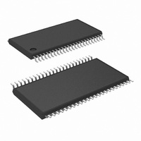
COP8CCE9IMT7/NOPB National Semiconductor, COP8CCE9IMT7/NOPB Datasheet - Page 20

COP8CCE9IMT7/NOPB
Manufacturer Part Number
COP8CCE9IMT7/NOPB
Description
MCU 8BIT FLASH 8K MEM 48-TSSOP
Manufacturer
National Semiconductor
Series
COP8™ 8Cr
Datasheet
1.I2C-CPEV.pdf
(80 pages)
Specifications of COP8CCE9IMT7/NOPB
Core Processor
COP8
Core Size
8-Bit
Speed
10MHz
Connectivity
Microwire/Plus (SPI), UART/USART
Peripherals
Brown-out Detect/Reset, POR, PWM, WDT
Number Of I /o
39
Program Memory Size
8KB (8K x 8)
Program Memory Type
FLASH
Ram Size
256 x 8
Voltage - Supply (vcc/vdd)
2.7 V ~ 5.5 V
Data Converters
A/D 16x10b
Oscillator Type
Internal
Operating Temperature
-40°C ~ 125°C
Package / Case
48-TSSOP
Data Bus Width
8 bit
Maximum Clock Frequency
10 MHz
Data Ram Size
256 B
On-chip Adc
10 bit, 16 channel
Number Of Programmable I/os
37
Number Of Timers
2
Height
0.9 mm
Interface Type
SPI, USART
Length
12.5 mm
Maximum Operating Temperature
+ 125 C
Minimum Operating Temperature
- 40 C
Supply Voltage (max)
5.5 V
Supply Voltage (min)
2.7 V
Width
6.1 mm
Lead Free Status / RoHS Status
Lead free / RoHS Compliant
Eeprom Size
-
Lead Free Status / Rohs Status
Details
Other names
COP8CCE9IMT7
www.national.com
10.0 Functional Description
10.4 DATA MEMORY SEGMENT RAM EXTENSION
Data memory address 0FF is used as a memory mapped
location for the Data Segment Address Register (S).
The data store memory is either addressed directly by a
single byte address within the instruction, or indirectly rela-
tive to the reference of the B, X, or SP pointers (each
contains a single-byte address). This single-byte address
allows an addressing range of 256 locations from 00 to FF
hex. The upper bit of this single-byte address divides the
data store memory into two separate sections as outlined
previously. With the exception of the RAM register memory
from address locations 00F0 – 00FF, all RAM memory is
memory mapped with the upper bit of the single-byte ad-
dress being equal to zero. This allows the upper bit of the
single-byte address to determine whether or not the base
address range (from 0000 – 00FF) is extended. If this upper
bit equals one (representing address range 0080 – 00FF),
then address extension does not take place. Alternatively, if
this upper bit equals zero, then the data segment extension
register S is used to extend the base address range from
0000 – 007F to XX00 – XX7F, where XX represents the 8
bits from the S register. Thus the 128-byte data segment
extensions are located from addresses 0100 – 017F for data
segment 1, 0200 – 027F for data segment 2, etc., up to FF00
0000 – 007F represents data segment 0.
Refer to Table 1, to determine available RAM segments for
this device.
Figure 7 illustrates how the S register data memory exten-
sion is used in extending the lower half of the base address
range (00 to 7F hex) into 256 data segments of 128 bytes
– FF7F for data segment 255. The base address range from
(Continued)
FIGURE 7. RAM Organization
20
each, with a total addressing range of 32 kbytes from XX00
to XX7F. This organization allows a total of 256 data seg-
ments of 128 bytes each with an additional upper base
segment of 128 bytes. Furthermore, all addressing modes
are available for all data segments. The S register must be
changed under program control to move from one data
segment (128 bytes) to another. However, the upper base
segment (containing the 16 memory registers, I/O registers,
control registers, etc.) is always available regardless of the
contents of the S register, since the upper base segment
(address range 0080 to 00FF) is independent of data seg-
ment extension.
The instructions that utilize the stack pointer (SP) always
reference the stack as part of the base segment (Segment
0), regardless of the contents of the S register. The S register
is not changed by these instructions. Consequently, the
stack (used with subroutine linkage and interrupts) is always
located in the base segment. The stack pointer will be initial-
ized to point at data memory location 006F as a result of
reset.
The 128 bytes of RAM contained in the base segment are
split between the lower and upper base segments. The first
112 bytes of RAM are resident from address 0000 to 006F in
the lower base segment, while the remaining 16 bytes of
RAM represent the 16 data memory registers located at
addresses 00F0 to 00FF of the upper base segment. No
RAM is located at the upper sixteen addresses (0070 to
007F) of the lower base segment.
Additional RAM beyond these initial 128 bytes, however, will
always be memory mapped in groups of 128 bytes (or less)
at the data segment address extensions (XX00 to XX7F) of
the lower base segment. The additional 128 bytes of RAM in
this device are memory mapped at address locations 0100
through 017F.
20022510


