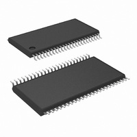
COP8CCE9IMT7/NOPB National Semiconductor, COP8CCE9IMT7/NOPB Datasheet - Page 64

COP8CCE9IMT7/NOPB
Manufacturer Part Number
COP8CCE9IMT7/NOPB
Description
MCU 8BIT FLASH 8K MEM 48-TSSOP
Manufacturer
National Semiconductor
Series
COP8™ 8Cr
Datasheet
1.I2C-CPEV.pdf
(80 pages)
Specifications of COP8CCE9IMT7/NOPB
Core Processor
COP8
Core Size
8-Bit
Speed
10MHz
Connectivity
Microwire/Plus (SPI), UART/USART
Peripherals
Brown-out Detect/Reset, POR, PWM, WDT
Number Of I /o
39
Program Memory Size
8KB (8K x 8)
Program Memory Type
FLASH
Ram Size
256 x 8
Voltage - Supply (vcc/vdd)
2.7 V ~ 5.5 V
Data Converters
A/D 16x10b
Oscillator Type
Internal
Operating Temperature
-40°C ~ 125°C
Package / Case
48-TSSOP
Data Bus Width
8 bit
Maximum Clock Frequency
10 MHz
Data Ram Size
256 B
On-chip Adc
10 bit, 16 channel
Number Of Programmable I/os
37
Number Of Timers
2
Height
0.9 mm
Interface Type
SPI, USART
Length
12.5 mm
Maximum Operating Temperature
+ 125 C
Minimum Operating Temperature
- 40 C
Supply Voltage (max)
5.5 V
Supply Voltage (min)
2.7 V
Width
6.1 mm
Lead Free Status / RoHS Status
Lead free / RoHS Compliant
Eeprom Size
-
Lead Free Status / Rohs Status
Details
Other names
COP8CCE9IMT7
www.national.com
18.0 MICROWIRE/PLUS
18.1.2.1 ALTERNATE SK PHASE OPERATION AND SK
IDLE POLARITY
The device allows either the normal SK clock or an alternate
phase SK clock to shift data in and out of the SIO register. In
both the modes the SK idle polarity can be either high or low.
The polarity is selected by bit 5 of Port G data register. In the
normal mode data is shifted in on the rising edge of the SK
clock and the data is shifted out on the falling edge of the SK
clock. The SIO register is shifted on each falling edge of the
SK Phase
Alternate
Alternate
Normal
Normal
FIGURE 34. MICROWIRE/PLUS SPI Mode Interface Timing, Alternate SK Mode, SK Idle Phase being Low
FIGURE 33. MICROWIRE/PLUS SPI Mode Interface Timing, Normal SK Mode, SK Idle Phase being Low
G6 (SKSEL)
Config. Bit
TABLE 32. MICROWIRE/PLUS Shift Clock Polarity and Sample/Shift Phase
0
1
0
1
Port G
(Continued)
G5 Data
Bit
0
0
1
1
SO Clocked Out On:
SK Falling Edge
SK Falling Edge
64
SK Rising Edge
SK Rising Edge
SK clock. In the alternate SK phase operation, data is shifted
in on the falling edge of the SK clock and shifted out on the
rising edge of the SK clock. Bit 6 of Port G configuration
register selects the SK edge.
A control flag, SKSEL, allows either the normal SK clock or
the alternate SK clock to be selected. Refer to Table 32 for
the appropriate setting of the SKSEL bit. The SKSEL is
mapped into the G6 configuration bit. The SKSEL flag will
power up in the reset condition, selecting the normal SK
signal provided the SK Idle Polarity remains LOW.
SI Sampled On:
SK Falling Edge
SK Falling Edge
SK Rising Edge
SK Rising Edge
20022536
20022537
SK Idle
Phase
High
High
Low
Low


