COP8CCE9IMT7/NOPB National Semiconductor, COP8CCE9IMT7/NOPB Datasheet - Page 23
COP8CCE9IMT7/NOPB
Manufacturer Part Number
COP8CCE9IMT7/NOPB
Description
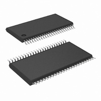
MCU 8BIT FLASH 8K MEM 48-TSSOP
Manufacturer
National Semiconductor
Series
COP8™ 8Cr
Datasheet
1.I2C-CPEV.pdf
(80 pages)
Specifications of COP8CCE9IMT7/NOPB
Core Processor
COP8
Core Size
8-Bit
Speed
10MHz
Connectivity
Microwire/Plus (SPI), UART/USART
Peripherals
Brown-out Detect/Reset, POR, PWM, WDT
Number Of I /o
39
Program Memory Size
8KB (8K x 8)
Program Memory Type
FLASH
Ram Size
256 x 8
Voltage - Supply (vcc/vdd)
2.7 V ~ 5.5 V
Data Converters
A/D 16x10b
Oscillator Type
Internal
Operating Temperature
-40°C ~ 125°C
Package / Case
48-TSSOP
Data Bus Width
8 bit
Maximum Clock Frequency
10 MHz
Data Ram Size
256 B
On-chip Adc
10 bit, 16 channel
Number Of Programmable I/os
37
Number Of Timers
2
Height
0.9 mm
Interface Type
SPI, USART
Length
12.5 mm
Maximum Operating Temperature
+ 125 C
Minimum Operating Temperature
- 40 C
Supply Voltage (max)
5.5 V
Supply Voltage (min)
2.7 V
Width
6.1 mm
Lead Free Status / RoHS Status
Lead free / RoHS Compliant
Eeprom Size
-
Lead Free Status / Rohs Status
Details
Other names
COP8CCE9IMT7


10.0 Functional Description
10.7.1 External Reset
The RESET input, when pulled low, initializes the device.
The RESET pin must be held low for a minimum of one
instruction cycle to guarantee a valid reset.
RESET may also be used to cause an exit from the HALT
mode.
A recommended reset circuit for this device is shown in
Figure 9.
(Continued)
WATCHDOG (if enabled):
The device comes out of reset with both the WATCHDOG
logic and the Clock Monitor detector armed, with the
WATCHDOG service window bits set and the Clock Moni-
tor bit set. The WATCHDOG and Clock Monitor circuits
are inhibited during reset. The WATCHDOG service win-
dow bits, being initialized high, default to the maximum
WATCHDOG service window of 64k T0 clock cycles. The
Clock Monitor bit being initialized high will cause a Clock
Monitor error following reset if the clock has not reached
the minimum specified frequency at the termination of
reset. A Clock Monitor error will cause an active low error
output on pin G1. This error output will continue until
16–32 T0 clock cycles following the clock frequency
reaching the minimum specified value, at which time the
G1 output will go high.
FIGURE 9. Reset Circuit Using External Reset
20022512
23
10.7.2 On-Chip Brownout Reset
When enabled, the device generates an internal reset as
V
voltage (V
the Idle Timer is preset with 00Fx (240–256 t
reaches a value greater than V
counting down. Upon underflow of the Idle Timer, the internal
reset is released and the device will start executing instruc-
tions. This internal reset will perform the same functions as
external reset. Once V
Timer time-out takes place, instruction execution begins and
the Idle Timer can be used normally. If, however, V
below the selected V
the Idle Timer is preset with 00Fx. The device now waits until
V
functional operation of the device, at frequency, is guaran-
teed down to the V
CC
CC
is greater than V
rises. While V
bor
), the device is held in the reset condition and
bor
CC
bor
bor
CC
level.
is less than the specified brownout
, an internal reset is generated, and
and the countdown starts over. The
is above the V
bor
, the Idle Timer starts
bor
and this initial Idle
C
). When V
www.national.com
CC
drops
CC
Related parts for COP8CCE9IMT7/NOPB
Image
Part Number
Description
Manufacturer
Datasheet
Request
R

Part Number:
Description:
National Semiconductor [8-Bit D/A Converter]
Manufacturer:
National Semiconductor
Datasheet:
Part Number:
Description:
National Semiconductor [Media Coprocessor]
Manufacturer:
National Semiconductor
Datasheet:
Part Number:
Description:
Digitally Controlled Tone and Volume Circuit with Stereo Audio Power Amplifier, Microphone Preamp Stage and National 3D Sound
Manufacturer:
National Semiconductor
Datasheet:
Part Number:
Description:
Digitally Controlled Tone and Volume Circuit with Stereo Audio Power Amplifier, Microphone Preamp Stage and National 3D Sound
Manufacturer:
National Semiconductor
Datasheet:
Part Number:
Description:
AC97 Rev 2 Codec with Sample Rate Conversion and National 3D Sound
Manufacturer:
National Semiconductor
Part Number:
Description:
Manufacturer:
National Semiconductor
Datasheet:
Part Number:
Description:
Manufacturer:
National Semiconductor
Datasheet:
Part Number:
Description:
General Purpose, Low Voltage, Low Power, Rail-to-Rail Output Operational Amplifiers
Manufacturer:
National Semiconductor
Datasheet:
Part Number:
Description:
8-bit 20 MSPS flash A/D converter.
Manufacturer:
National Semiconductor
Datasheet:
Part Number:
Description:
Low Noise Quad Operational Amplifier
Manufacturer:
National Semiconductor
Datasheet:
Part Number:
Description:
Quad Differential Line Receivers
Manufacturer:
National Semiconductor
Datasheet:
Part Number:
Description:
Quad High Speed Trapezoidal? Bus Transceiver
Manufacturer:
National Semiconductor
Datasheet:
Part Number:
Description:
Dual Line Receiver
Manufacturer:
National Semiconductor
Datasheet:
Part Number:
Description:
TTL to 10k ECL Level Translator with Latch
Manufacturer:
National Semiconductor
Datasheet: