COP8CCE9IMT7/NOPB National Semiconductor, COP8CCE9IMT7/NOPB Datasheet - Page 21
COP8CCE9IMT7/NOPB
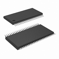
Manufacturer Part Number
COP8CCE9IMT7/NOPB
Description
MCU 8BIT FLASH 8K MEM 48-TSSOP
Manufacturer
National Semiconductor
Series
COP8™ 8Cr
Datasheet
1.I2C-CPEV.pdf
(80 pages)
Specifications of COP8CCE9IMT7/NOPB
Core Processor
COP8
Core Size
8-Bit
Speed
10MHz
Connectivity
Microwire/Plus (SPI), UART/USART
Peripherals
Brown-out Detect/Reset, POR, PWM, WDT
Number Of I /o
39
Program Memory Size
8KB (8K x 8)
Program Memory Type
FLASH
Ram Size
256 x 8
Voltage - Supply (vcc/vdd)
2.7 V ~ 5.5 V
Data Converters
A/D 16x10b
Oscillator Type
Internal
Operating Temperature
-40°C ~ 125°C
Package / Case
48-TSSOP
Data Bus Width
8 bit
Maximum Clock Frequency
10 MHz
Data Ram Size
256 B
On-chip Adc
10 bit, 16 channel
Number Of Programmable I/os
37
Number Of Timers
2
Height
0.9 mm
Interface Type
SPI, USART
Length
12.5 mm
Maximum Operating Temperature
+ 125 C
Minimum Operating Temperature
- 40 C
Supply Voltage (max)
5.5 V
Supply Voltage (min)
2.7 V
Width
6.1 mm
Lead Free Status / RoHS Status
Lead free / RoHS Compliant
Eeprom Size
-
Lead Free Status / Rohs Status
Details
Other names
COP8CCE9IMT7


10.0 Functional Description
10.4.1 Virtual EEPROM
The Flash memory and the User ISP functions (see Section
5.7), provide the user with the capability to use the flash
program memory to back up user defined sections of RAM.
This effectively provides the user with the same nonvolatile
data storage as EEPROM. Management, and even the
amount of memory used, are the responsibility of the user,
however the flash memory read and write functions have
been provided in the boot ROM.
One typical method of using the Virtual EEPROM feature
would be for the user to copy the data to RAM during system
initialization, periodically, and if necessary, erase the page of
Flash and copy the contents of the RAM back to the Flash.
10.5 OPTION REGISTER
The Option register, located at address 0x3FFF (hex) in the
Flash Program Memory, is used to configure the user select-
able security, WATCHDOG, and HALT options. The register
can be programmed only in external Flash Memory program-
ming or ISP Programming modes. Therefore, the register
must be programmed at the same time as the program
memory. The contents of the Option register shipped from
the factory read 00 Hex.
The format of the Option register is as follows:
Bits 7, 6 These bits are reserved and must be 0.
Bit 5
Bits 4, 3 These bits are reserved and must be 0.
Bit 2
Bit 1
Bit 0
The COP8 assembler defines a special ROM section type,
CONF, into which the Option Register data may be coded.
The Option Register is programmed automatically by pro-
grammers that are certified by National.
The user needs to ensure that the FLEX bit will be set when
the device is programmed.
The following examples illustrate the declaration of the Op-
tion Register.
Syntax:
(Continued)
Bit 7
= 1
= 0
= 1
= 0
= 1
= 0
= 1
= 0
Reserved
Bit 6
Security enabled. Flash Memory read and write
are not allowed except in User ISP/Virtual E
mands. Mass Erase is allowed.
Security disabled. Flash Memory read and write
are allowed.
WATCHDOG feature disabled. G1 is a general
purpose I/O.
WATCHDOG
WATCHDOG output with weak pullup.
HALT mode disabled.
HALT mode enabled.
Execution following RESET will be from Flash
Memory.
Flash Memory is erased. Execution following RE-
SET will be from Boot ROM with the MICROWIRE/
PLUS ISP routines.
SECURITY
Bit 5
Bit 4
feature
Reserved
Bit 3
enabled.
WATCH
Bit 2
DOG
HALT
Bit 1
G1
pin
2
FLEX
Bit 0
com-
is
21
[label:].sect
Example: The following sets a value in the Option Register
and User Identification for a COP8CBE9HVA7. The Option
Register bit values shown select options: Security disabled,
WATCHDOG enabled HALT mode enabled and execution
will commence from Flash Memory.
Note: All programmers certified for programming this family
of parts will support programming of the Option Register.
Please contact National or your device programmer supplier
for more information.
10.6 SECURITY
The device has a security feature which, when enabled,
prevents external reading of the Flash program memory. The
security bit in the Option Register determines, whether se-
curity is enabled or disabled. If the security feature is dis-
abled, the contents of the internal Flash Memory may be
read by external programmers or by the built in
MICROWIRE/PLUS serial interface ISP. Security must be
enforced by the user when the contents of the Flash
Memory are accessed via the user ISP or Virtual EE-
PROM capability.
If the security feature is enabled, then any attempt to exter-
nally read the contents of the Flash Memory will result in the
value FF (hex) being read from all program locations (except
the Option Register). In addition, with the security feature
enabled, the write operation to the Flash program memory
and Option Register is inhibited. Page Erases are also inhib-
ited when the security feature is enabled. The Option Reg-
ister is readable regardless of the state of the security bit by
accessing location FFFF (hex). Mass Erase Operations are
possible regardless of the state of the security bit.
The security bit can be erased only by a Mass Erase of the
entire contents of the Flash unless Flash operation is under
the control of User ISP functions.
Note: The actual memory address of the Option Register is
0x3FFF (hex), however the MICROWIRE/PLUS ISP routines
require the address FFFF (hex) to be used to read the
Option Register when the Flash Memory is secured.
The entire Option Register must be programmed at one time
and cannot be rewritten without first erasing the entire last
page of Flash Memory.
.chip
.sect
.db
.endsect
...
.end
.db
.endsect
8CBE
option, conf
0x01
start
config, conf
value
;wd, halt, flex
;1 byte,
;configures
;options
www.national.com
Related parts for COP8CCE9IMT7/NOPB
Image
Part Number
Description
Manufacturer
Datasheet
Request
R

Part Number:
Description:
National Semiconductor [8-Bit D/A Converter]
Manufacturer:
National Semiconductor
Datasheet:
Part Number:
Description:
National Semiconductor [Media Coprocessor]
Manufacturer:
National Semiconductor
Datasheet:
Part Number:
Description:
Digitally Controlled Tone and Volume Circuit with Stereo Audio Power Amplifier, Microphone Preamp Stage and National 3D Sound
Manufacturer:
National Semiconductor
Datasheet:
Part Number:
Description:
Digitally Controlled Tone and Volume Circuit with Stereo Audio Power Amplifier, Microphone Preamp Stage and National 3D Sound
Manufacturer:
National Semiconductor
Datasheet:
Part Number:
Description:
AC97 Rev 2 Codec with Sample Rate Conversion and National 3D Sound
Manufacturer:
National Semiconductor
Part Number:
Description:
Manufacturer:
National Semiconductor
Datasheet:
Part Number:
Description:
Manufacturer:
National Semiconductor
Datasheet:
Part Number:
Description:
General Purpose, Low Voltage, Low Power, Rail-to-Rail Output Operational Amplifiers
Manufacturer:
National Semiconductor
Datasheet:
Part Number:
Description:
8-bit 20 MSPS flash A/D converter.
Manufacturer:
National Semiconductor
Datasheet:
Part Number:
Description:
Low Noise Quad Operational Amplifier
Manufacturer:
National Semiconductor
Datasheet:
Part Number:
Description:
Quad Differential Line Receivers
Manufacturer:
National Semiconductor
Datasheet:
Part Number:
Description:
Quad High Speed Trapezoidal? Bus Transceiver
Manufacturer:
National Semiconductor
Datasheet:
Part Number:
Description:
Dual Line Receiver
Manufacturer:
National Semiconductor
Datasheet:
Part Number:
Description:
TTL to 10k ECL Level Translator with Latch
Manufacturer:
National Semiconductor
Datasheet: