COP8CCE9IMT7/NOPB National Semiconductor, COP8CCE9IMT7/NOPB Datasheet - Page 66
COP8CCE9IMT7/NOPB
Manufacturer Part Number
COP8CCE9IMT7/NOPB
Description
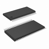
MCU 8BIT FLASH 8K MEM 48-TSSOP
Manufacturer
National Semiconductor
Series
COP8™ 8Cr
Datasheet
1.I2C-CPEV.pdf
(80 pages)
Specifications of COP8CCE9IMT7/NOPB
Core Processor
COP8
Core Size
8-Bit
Speed
10MHz
Connectivity
Microwire/Plus (SPI), UART/USART
Peripherals
Brown-out Detect/Reset, POR, PWM, WDT
Number Of I /o
39
Program Memory Size
8KB (8K x 8)
Program Memory Type
FLASH
Ram Size
256 x 8
Voltage - Supply (vcc/vdd)
2.7 V ~ 5.5 V
Data Converters
A/D 16x10b
Oscillator Type
Internal
Operating Temperature
-40°C ~ 125°C
Package / Case
48-TSSOP
Data Bus Width
8 bit
Maximum Clock Frequency
10 MHz
Data Ram Size
256 B
On-chip Adc
10 bit, 16 channel
Number Of Programmable I/os
37
Number Of Timers
2
Height
0.9 mm
Interface Type
SPI, USART
Length
12.5 mm
Maximum Operating Temperature
+ 125 C
Minimum Operating Temperature
- 40 C
Supply Voltage (max)
5.5 V
Supply Voltage (min)
2.7 V
Width
6.1 mm
Lead Free Status / RoHS Status
Lead free / RoHS Compliant
Eeprom Size
-
Lead Free Status / Rohs Status
Details
Other names
COP8CCE9IMT7


www.national.com
19.0 Memory Map
xxC5
xxC6
xxC7
xxC8
xxC9
xxCA
xxCB
xxCC
xxCD
xxCE
xxCF
xxD0
xxD1
xxD2
xxD3
xxD4
xxD5
xxD6
xxD7 to xxDB
xxDC
xxDD
xxDE
xxDF
xxE0
xxE1
xxE2
xxE3 to xxE5
xxE6
xxE7
xxE8
xxE9
xxEA
xxEB
xxEC
xxED
xxEE
xxEF
xxF0 to FB
xxFC
S/ADD REG
Address
Timer T2 Autoload Register T2RB Upper
Byte
Timer T2 Control Register
WATCHDOG Service Register
(Reg:WDSVR)
MIWU Edge Select Register
(Reg:WKEDG)
MIWU Enable Register (Reg:WKEN)
MIWU Pending Register (Reg:WKPND)
A/D Converter Control Register (ENAD)
A/D Converter Result Register High Byte
(ADRSTH)
A/D Converter Result Register Low Byte
(ADRSTL)
Reserved
Idle Timer Control Register (ITMR)
Port L Data Register
Port L Configuration Register
Port L Input Pins (Read Only)
Reserved for Port L
Port G Data Register
Port G Configuration Register
Port G Input Pins (Read Only)
Reserved
Port H Data Register
Port H Configuration Register
Port H Input Pins (Read Only)
Reserved for Port H
Reserved
Flash Memory Write Timing Register
(PGMTIM)
ISP Key Register (ISPKEY)
Reserved
Timer T1 Autoload Register T1RB Lower
Byte
Timer T1 Autoload Register T1RB Upper
Byte
ICNTRL Register
MICROWIRE/PLUS Shift Register
Timer T1 Lower Byte
Timer T1 Upper Byte
Timer T1 Autoload Register T1RA Lower
Byte
Timer T1 Autoload Register T1RA Upper
Byte
CNTRL Control Register
PSW Register
On-Chip RAM Mapped as Registers
X Register
(Continued)
Contents
66
Note: Reading memory locations 0070H–007FH (Segment 0) will return all
20.0 Instruction Set
20.1 INTRODUCTION
This section defines the instruction set of the COP8 Family
members. It contains information about the instruction set
features, addressing modes and types.
20.2 INSTRUCTION FEATURES
The strength of the instruction set is based on the following
features:
• Mostly single-byte opcode instructions minimize program
• One instruction cycle for the majority of single-byte in-
• Many single-byte, multiple function instructions such as
• Three memory mapped pointers: two for register indirect
• Sixteen memory mapped registers that allow an opti-
• Ability to set, reset, and test any individual bit in data
• Register-Indirect LOAD and EXCHANGE instructions
• Unique instructions to optimize program size and
20.3 ADDRESSING MODES
The instruction set offers a variety of methods for specifying
memory addresses. Each method is called an addressing
mode. These modes are classified into two categories: op-
erand addressing modes and transfer-of-control addressing
modes. Operand addressing modes are the various meth-
ods of specifying an address for accessing (reading or writ-
ing) data. Transfer-of-control addressing modes are used in
conjunction with jump instructions to control the execution
sequence of the software program.
20.3.1 Operand Addressing Modes
The operand of an instruction specifies what memory loca-
tion is to be affected by that instruction. Several different
operand addressing modes are available, allowing memory
locations to be specified in a variety of ways. An instruction
can specify an address directly by supplying the specific
address, or indirectly by specifying a register pointer. The
contents of the register (or in some cases, two registers)
xxFD
xxFE
xxFF
0100 to 017F
S/ADD REG
size.
structions to minimize program execution time.
DRSZ.
addressing, and one for the software stack.
mized implementation of certain instructions.
memory address space, including the memory-mapped
I/O ports and registers.
with optional automatic post-incrementing or decrement-
ing of the register pointer. This allows for greater effi-
ciency (both in cycle time and program code) in loading,
walking across and processing fields in data memory.
throughput efficiency. Some of these instructions are:
DRSZ, IFBNE, DCOR, RETSK, VIS and RRC.
Address
ones. Reading unused memory locations 0080H–0093H (Segment 0)
will return undefined data. Reading memory locations from other Seg-
ments (i.e., Segment 8, Segment 9, … etc.) will return undefined data.
SP Register
B Register
S Register
On-Chip 128 RAM Bytes
Contents
Related parts for COP8CCE9IMT7/NOPB
Image
Part Number
Description
Manufacturer
Datasheet
Request
R

Part Number:
Description:
National Semiconductor [8-Bit D/A Converter]
Manufacturer:
National Semiconductor
Datasheet:
Part Number:
Description:
National Semiconductor [Media Coprocessor]
Manufacturer:
National Semiconductor
Datasheet:
Part Number:
Description:
Digitally Controlled Tone and Volume Circuit with Stereo Audio Power Amplifier, Microphone Preamp Stage and National 3D Sound
Manufacturer:
National Semiconductor
Datasheet:
Part Number:
Description:
Digitally Controlled Tone and Volume Circuit with Stereo Audio Power Amplifier, Microphone Preamp Stage and National 3D Sound
Manufacturer:
National Semiconductor
Datasheet:
Part Number:
Description:
AC97 Rev 2 Codec with Sample Rate Conversion and National 3D Sound
Manufacturer:
National Semiconductor
Part Number:
Description:
Manufacturer:
National Semiconductor
Datasheet:
Part Number:
Description:
Manufacturer:
National Semiconductor
Datasheet:
Part Number:
Description:
General Purpose, Low Voltage, Low Power, Rail-to-Rail Output Operational Amplifiers
Manufacturer:
National Semiconductor
Datasheet:
Part Number:
Description:
8-bit 20 MSPS flash A/D converter.
Manufacturer:
National Semiconductor
Datasheet:
Part Number:
Description:
Low Noise Quad Operational Amplifier
Manufacturer:
National Semiconductor
Datasheet:
Part Number:
Description:
Quad Differential Line Receivers
Manufacturer:
National Semiconductor
Datasheet:
Part Number:
Description:
Quad High Speed Trapezoidal? Bus Transceiver
Manufacturer:
National Semiconductor
Datasheet:
Part Number:
Description:
Dual Line Receiver
Manufacturer:
National Semiconductor
Datasheet:
Part Number:
Description:
TTL to 10k ECL Level Translator with Latch
Manufacturer:
National Semiconductor
Datasheet: