COP8CCE9IMT7/NOPB National Semiconductor, COP8CCE9IMT7/NOPB Datasheet - Page 29
COP8CCE9IMT7/NOPB
Manufacturer Part Number
COP8CCE9IMT7/NOPB
Description
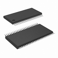
MCU 8BIT FLASH 8K MEM 48-TSSOP
Manufacturer
National Semiconductor
Series
COP8™ 8Cr
Datasheet
1.I2C-CPEV.pdf
(80 pages)
Specifications of COP8CCE9IMT7/NOPB
Core Processor
COP8
Core Size
8-Bit
Speed
10MHz
Connectivity
Microwire/Plus (SPI), UART/USART
Peripherals
Brown-out Detect/Reset, POR, PWM, WDT
Number Of I /o
39
Program Memory Size
8KB (8K x 8)
Program Memory Type
FLASH
Ram Size
256 x 8
Voltage - Supply (vcc/vdd)
2.7 V ~ 5.5 V
Data Converters
A/D 16x10b
Oscillator Type
Internal
Operating Temperature
-40°C ~ 125°C
Package / Case
48-TSSOP
Data Bus Width
8 bit
Maximum Clock Frequency
10 MHz
Data Ram Size
256 B
On-chip Adc
10 bit, 16 channel
Number Of Programmable I/os
37
Number Of Timers
2
Height
0.9 mm
Interface Type
SPI, USART
Length
12.5 mm
Maximum Operating Temperature
+ 125 C
Minimum Operating Temperature
- 40 C
Supply Voltage (max)
5.5 V
Supply Voltage (min)
2.7 V
Width
6.1 mm
Lead Free Status / RoHS Status
Lead free / RoHS Compliant
Eeprom Size
-
Lead Free Status / Rohs Status
Details
Other names
COP8CCE9IMT7


11.0 In-System Programming
11.4 MANEUVERING BACK AND FORTH BETWEEN
FLASH MEMORY AND BOOT ROM
When using ISP, at some point, it will be necessary to
maneuver between the flash program memory and the Boot
ROM, even when using customized ISP routines. This is
because it’s not possible to execute from the flash program
memory while it’s being programmed.
Two instructions are available to perform the task of jumping
back and forth: Jump to Boot (JSRB) and Return to Flash
(RETF). The JSRB instruction is used to jump from flash
memory to Boot ROM, and the RETF is used to return from
the Boot ROM back to the flash program memory. See
Section 20.0 Instruction Set for specific details on the opera-
tion of these instructions.
The JSRB instruction must be used in conjunction with the
Key register. This is to prevent jumping to the Boot ROM in
the event of run-away software. For the JSRB instruction to
actually jump to the Boot ROM, the Key bit must be set. This
is done by writing the value shown in Table 9 to the Key
register. The Key is a 6 bit key and if the key matches, the
KEY bit will be set for 8 instruction cycles. The JSRB instruc-
tion must be executed while the KEY bit is set. If the KEY
does not match, then the KEY bit will not be set and the
JSRB will jump to the specified location in the flash memory.
In emulation mode, if a breakpoint is encountered while the
KEY is set, the counter that counts the instruction cycles will
be frozen until the breakpoint condition is cleared. If an
interrupt occurs while the key is set, the key will expire
before interrupt service is complete. It is recommended
that the software globally disable interrupts before set-
ting the key and re-enable interrupts on completion of
Boot ROM execution. The Key register is a memory
mapped register. Its format when writing is shown in Table 9.
Bits 7–2: Key value that must be written to set the KEY bit.
Bits 1–0: Don’t care.
11.5 FORCED EXECUTION FROM BOOT ROM
When the user is developing a customized ISP routine, code
lockups due to software errors may be encountered. The
normal, and preferred, method to recover from these condi-
Bit 7
R
7
0
0
0
0
0
0
0
0
1
Bit 6
0
TABLE 9. KEY Register Write Format
R/W
6
1
1
1
1
1
1
1
1
Bit 5
0
KEY When Writing
Bit 4
R/W
1
5
0
0
0
0
0
1
1
1
Bit 3
1
R/W
TABLE 8. PGMTIM Register Format (Continued)
Bit 2
4
0
0
0
1
1
0
0
1
Register Bit
0
Bit 1
X
R/W
(Continued)
3
1
1
1
0
1
0
1
1
Bit 0
X
PGMTIM
R/W
29
2
0
0
1
1
0
0
1
0
tions is to reprogram the device with the corrected code by
either an external parallel programmer or the emulation
tools. As a last resort, when this equipment is not available,
there is a hardware method to get out of these lockups and
force execution from the Boot ROM MICROWIRE/PLUS
routine. The customer will then be able to erase the Flash
Memory code and start over.
The method to force this condition is to drive the G6 pin to
high voltage (2 x V
condition on G6 must not be applied before V
stable, and must be held for at least 3 instruction cycles
longer than Reset is active. This special condition will by-
pass checking the state of the Flex bit in the Option Register
and will start execution from location 0000 in the Boot ROM.
In this state, the user can input the appropriate commands,
using MICROWIRE/PLUS, to erase the flash program
memory and reprogram it. If the device is subsequently reset
before the Flex bit has been erased by specific Page Erase
or Mass Erase ISP commands, execution will start from
location 0000 in the Flash program memory. The high volt-
age (2 x V
Security bit in the Option Register. The Security bit, if set,
can only be erased by a Mass Erase of the entire contents of
the Flash Memory unless under the control of User ISP
routines in the Application Program.
While the G6 pin is at high voltage, the Load Clock will be
output onto G5, which will look like an SK clock to the
MICROWIRE/PLUS routine executing in slave mode. How-
ever, when G6 is at high voltage, the G6 input will also look
like a logic 1. The MICROWIRE/PLUS routine in Boot ROM
monitors the G6 input, waits for it to go low, debounces it,
and then enables the ISP routine. CAUTION: The Load clock
on G5 could be in conflict with the user’s external SK. It is up
to the user to resolve this conflict, as this condition is con-
sidered a minor issue that’s only encountered during soft-
ware development. The user should also be cautious of
the high voltage applied to the G6 pin. This high voltage
could damage other circuitry connected to the G6 pin
(e.g. the parallel port of a PC). The user may wish to
disconnect other circuitry while G6 is connected to the high
voltage.
V
to G6.
CC
must be valid and stable before high voltage is applied
R/W
1
0
1
1
0
1
1
1
1
CC
) on G6 will not erase either the Flex or the
CC
R/W
0
0
1
1
0
1
1
1
1
) and activate Reset. The high voltage
CKI Frequency Range
1.125 MHz–1.5 MHz
2.625 MHz–3.5 MHz
3.5 MHz–4.67 MHz
2 MHz–2.67 MHz
7.5 MHz–10 MHz
1.5 MHz–2 MHz
4.5 MHz–6 MHz
6 MHz–8 MHz
CC
www.national.com
is valid and
Related parts for COP8CCE9IMT7/NOPB
Image
Part Number
Description
Manufacturer
Datasheet
Request
R

Part Number:
Description:
National Semiconductor [8-Bit D/A Converter]
Manufacturer:
National Semiconductor
Datasheet:
Part Number:
Description:
National Semiconductor [Media Coprocessor]
Manufacturer:
National Semiconductor
Datasheet:
Part Number:
Description:
Digitally Controlled Tone and Volume Circuit with Stereo Audio Power Amplifier, Microphone Preamp Stage and National 3D Sound
Manufacturer:
National Semiconductor
Datasheet:
Part Number:
Description:
Digitally Controlled Tone and Volume Circuit with Stereo Audio Power Amplifier, Microphone Preamp Stage and National 3D Sound
Manufacturer:
National Semiconductor
Datasheet:
Part Number:
Description:
AC97 Rev 2 Codec with Sample Rate Conversion and National 3D Sound
Manufacturer:
National Semiconductor
Part Number:
Description:
Manufacturer:
National Semiconductor
Datasheet:
Part Number:
Description:
Manufacturer:
National Semiconductor
Datasheet:
Part Number:
Description:
General Purpose, Low Voltage, Low Power, Rail-to-Rail Output Operational Amplifiers
Manufacturer:
National Semiconductor
Datasheet:
Part Number:
Description:
8-bit 20 MSPS flash A/D converter.
Manufacturer:
National Semiconductor
Datasheet:
Part Number:
Description:
Low Noise Quad Operational Amplifier
Manufacturer:
National Semiconductor
Datasheet:
Part Number:
Description:
Quad Differential Line Receivers
Manufacturer:
National Semiconductor
Datasheet:
Part Number:
Description:
Quad High Speed Trapezoidal? Bus Transceiver
Manufacturer:
National Semiconductor
Datasheet:
Part Number:
Description:
Dual Line Receiver
Manufacturer:
National Semiconductor
Datasheet:
Part Number:
Description:
TTL to 10k ECL Level Translator with Latch
Manufacturer:
National Semiconductor
Datasheet: