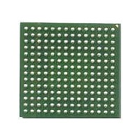
MCF5272VM66J Freescale Semiconductor, MCF5272VM66J Datasheet - Page 150

MCF5272VM66J
Manufacturer Part Number
MCF5272VM66J
Description
IC MCU 166MHZ 196MAPBGA
Manufacturer
Freescale Semiconductor
Series
MCF527xr
Datasheets
1.MCF5272CVF66J.pdf
(544 pages)
2.MCF5272CVF66J.pdf
(12 pages)
3.MCF5272VM66J.pdf
(44 pages)
Specifications of MCF5272VM66J
Core Processor
Coldfire V2
Core Size
32-Bit
Speed
66MHz
Connectivity
EBI/EMI, Ethernet, I²C, SPI, UART/USART, USB
Peripherals
DMA, WDT
Number Of I /o
32
Program Memory Size
16KB (4K x 32)
Program Memory Type
ROM
Ram Size
1K x 32
Voltage - Supply (vcc/vdd)
3 V ~ 3.6 V
Oscillator Type
External
Operating Temperature
0°C ~ 70°C
Package / Case
196-MAPBGA
Processor Series
MCF527x
Core
ColdFire V2
Data Bus Width
32 bit
Data Ram Size
64 KB
Interface Type
I2C, UART, Ethernet, SPI, USB, QSPI
Maximum Clock Frequency
166 MHz
Number Of Timers
4
Operating Supply Voltage
1.4 V to 1.6 V
Maximum Operating Temperature
+ 85 C
Mounting Style
SMD/SMT
3rd Party Development Tools
JLINK-CF-BDM26, EWCF
Development Tools By Supplier
NNDK-MOD5272-KIT, NNDK-MOD5270-KIT
Minimum Operating Temperature
- 40 C
Lead Free Status / RoHS Status
Lead free / RoHS Compliant
Eeprom Size
-
Data Converters
-
Lead Free Status / Rohs Status
Lead free / RoHS Compliant
Available stocks
Company
Part Number
Manufacturer
Quantity
Price
Company:
Part Number:
MCF5272VM66J
Manufacturer:
FREESCAL
Quantity:
416
Company:
Part Number:
MCF5272VM66J
Manufacturer:
Freescale
Quantity:
178
Company:
Part Number:
MCF5272VM66J
Manufacturer:
Freescale Semiconductor
Quantity:
10 000
- Current page: 150 of 544
- Download datasheet (7Mb)
Debug Support
Operand Data:
Result Data:
5.5.3.3.11
Read the selected debug module register and return the 32-bit result. The only valid register selection for
the
BKPT]; as well as the trigger status bits (CSR[BSTAT]) if either a level-2 breakpoint has been triggered
or a level-1 breakpoint has been triggered and no level-2 breakpoint has been enabled.
Command/Result Formats:
Table 5-20
Command Sequence:
Operand Data:
Result Data:
5-32
RDMREG
Command
0x01–0x1F
DRc[4:0]
0x00
Result
shows the definition of DRc encoding.
command is CSR (DRc = 0x00). Note that this read of the CSR clears CSR[FOF, TRG, HALT,
Read Debug Module Register (
15
MCF5272 ColdFire
This instruction requires two longword operands. The first selects the register to
which the operand data is to be written; the second contains the data.
Successful write operations return 0xFFFF. Bus errors on the write cycle are
indicated by the setting of bit 16 in the status message and by a data pattern of
0x0001.
None
The contents of the selected debug register are returned as a longword value. The
data is returned most-significant word first.
Debug Register Definition
0x2
Figure 5-37.
Configuration/Status
Table 5-20. Definition of DRc Encoding—Read
Reserved
Figure 5-38.
RDMREG
12
???
®
11
RDMREG BDM
Integrated Microprocessor User’s Manual, Rev. 3
RDMREG
0xD
MS RESULT
"ILLEGAL"
RDMREG
Command/Result Formats
Command Sequence
XXX
XXX
D[31:16]
8
D[15:0]
Mnemonic
7
)
CSR
—
100
"NOT READY"
LS RESULT
NEXT CMD
NEXT CMD
5
Initial State
4
0x0
—
Freescale Semiconductor
DRc
p. 5-10
Page
—
0
Related parts for MCF5272VM66J
Image
Part Number
Description
Manufacturer
Datasheet
Request
R
Part Number:
Description:
Mcf5272 Coldfire Integrated Microprocessor User
Manufacturer:
Freescale Semiconductor, Inc
Datasheet:

Part Number:
Description:
MCF5272 Interrupt Service Routine for the Physical Layer Interface Controller
Manufacturer:
Freescale Semiconductor / Motorola
Datasheet:
Part Number:
Description:
Manufacturer:
Freescale Semiconductor, Inc
Datasheet:
Part Number:
Description:
Manufacturer:
Freescale Semiconductor, Inc
Datasheet:
Part Number:
Description:
Manufacturer:
Freescale Semiconductor, Inc
Datasheet:
Part Number:
Description:
Manufacturer:
Freescale Semiconductor, Inc
Datasheet:
Part Number:
Description:
Manufacturer:
Freescale Semiconductor, Inc
Datasheet:
Part Number:
Description:
Manufacturer:
Freescale Semiconductor, Inc
Datasheet:
Part Number:
Description:
Manufacturer:
Freescale Semiconductor, Inc
Datasheet:
Part Number:
Description:
Manufacturer:
Freescale Semiconductor, Inc
Datasheet:
Part Number:
Description:
Manufacturer:
Freescale Semiconductor, Inc
Datasheet:
Part Number:
Description:
Manufacturer:
Freescale Semiconductor, Inc
Datasheet:
Part Number:
Description:
Manufacturer:
Freescale Semiconductor, Inc
Datasheet:
Part Number:
Description:
Manufacturer:
Freescale Semiconductor, Inc
Datasheet:
Part Number:
Description:
Manufacturer:
Freescale Semiconductor, Inc
Datasheet:


