SAK-C164CM-4EF AB Infineon Technologies, SAK-C164CM-4EF AB Datasheet - Page 11
SAK-C164CM-4EF AB
Manufacturer Part Number
SAK-C164CM-4EF AB
Description
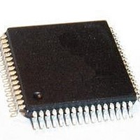
IC MCU 16BIT 32KB OTP TQFP-64-4
Manufacturer
Infineon Technologies
Series
C16xxr
Datasheet
1.SAF-C164CM-4EF_AB.pdf
(68 pages)
Specifications of SAK-C164CM-4EF AB
Core Processor
C166
Core Size
16-Bit
Speed
20MHz
Connectivity
CAN, EBI/EMI, SPI, UART/USART
Peripherals
POR, PWM, WDT
Number Of I /o
50
Program Memory Size
32KB (32K x 8)
Program Memory Type
OTP
Ram Size
2K x 8
Voltage - Supply (vcc/vdd)
4.5 V ~ 5.5 V
Data Converters
A/D 8x10b
Oscillator Type
External
Operating Temperature
-40°C ~ 125°C
Package / Case
64-LFQFP
Data Bus Width
16 bit
Data Ram Size
2 KB
Interface Type
1xASC, 1xSSC
Maximum Clock Frequency
20 MHz
Number Of Programmable I/os
50
Number Of Timers
5
Operating Supply Voltage
5 V
Maximum Operating Temperature
+ 125 C
Mounting Style
SMD/SMT
Minimum Operating Temperature
- 40 C
On-chip Adc
10 bit, 8 Channel
Packages
P-TQFP-64
Max Clock Frequency
20.0 MHz
Sram (incl. Cache)
2.0 KByte
Can Nodes
1
A / D Input Lines (incl. Fadc)
8
Program Memory
32.0 KByte
Lead Free Status / RoHS Status
Lead free / RoHS Compliant
Eeprom Size
-
Lead Free Status / Rohs Status
Details
Other names
SAK-C164CM-4EFAB
SAK-C164CM-4EFABINTR
SAK-C164CM-4EFABTR
SAK-C164CM-4EFABTR
SAKC164CM4EFABXT
SP000056829
SP000104063
SAK-C164CM-4EFABINTR
SAK-C164CM-4EFABTR
SAK-C164CM-4EFABTR
SAKC164CM4EFABXT
SP000056829
SP000104063


Table 2
Symbol Pin
P20
P20.0
P20.1
P20.4
P20.5
P20.8
P20.12
Data Sheet
No.
28
29
30
31
34
35
Pin Definitions and Functions (cont’d)
Input
Outp.
IO
O
O
O
I
–
O
O
O
Function
Port 20 is a 6-bit bidirectional I/O port (no P20.5 output driver
in the OTP versions). It is bit-wise programmable for input or
output via direction bits. For a pin configured as input, the
output driver is put into high-impedance state.
The following Port 20 pins also serve for alternate functions:
RD
WR
ALE
Can be used for latching the address into external memory
or an address latch in the multiplexed bus modes.
EA
A low level at this pin during and after Reset forces the
C164CM to latch the configuration from PORT0 and pin RD,
and to begin instruction execution out of external memory.
A high level forces the C164CM to latch the configuration
from pins RD, ALE, and WR, and to begin instruction
execution out of the internal program memory.
“ROMless” versions must have this pin tied to ‘0’.
V
The OTP versions of the C164CM receive the programming
voltage via this pin. (No output driver for P20.5 in this case!)
CLKOUT
FOUT
RSTOUT
to a low level when the part is executing either a hardware-,
a software- or a watchdog timer reset. RSTOUT remains low
until the EINIT (end of initialization) instruction is executed.
PP
External Memory Read Strobe, activated for
every external instruction or data read access.
External Memory Write Strobe, activated for
every external data write access.
Address Latch Enable Output.
External Access Enable pin.
OTP Programming voltage
System Clock Output (= CPU Clock),
Programmable Frequency Output
Internal Reset Indication Output. This pin is set
7
V1.0, 2001-05
C164CM
C164SM
Related parts for SAK-C164CM-4EF AB
Image
Part Number
Description
Manufacturer
Datasheet
Request
R


Part Number:
Description:
16-Bit Single-Chip Microcontrol ler
Manufacturer:
Infineon Technologies AG
Datasheet:
Part Number:
Description:
Manufacturer:
Infineon Technologies AG
Datasheet:
Part Number:
Description:
Manufacturer:
Infineon Technologies AG
Datasheet:
Part Number:
Description:
Manufacturer:
Infineon Technologies AG
Datasheet:
Part Number:
Description:
Manufacturer:
Infineon Technologies AG
Datasheet:
Part Number:
Description:
Manufacturer:
Infineon Technologies AG
Datasheet:
Part Number:
Description:
Manufacturer:
Infineon Technologies AG
Datasheet:
Part Number:
Description:
Manufacturer:
Infineon Technologies AG
Datasheet:
Part Number:
Description:
16-bit microcontroller with 2x2 KByte RAM
Manufacturer:
Infineon Technologies AG
Datasheet:
Part Number:
Description:
NPN silicon RF transistor
Manufacturer:
Infineon Technologies AG
Datasheet:
Part Number:
Description:
NPN silicon RF transistor
Manufacturer:
Infineon Technologies AG
Datasheet:
Part Number:
Description:
NPN silicon RF transistor
Manufacturer:
Infineon Technologies AG
Datasheet:
Part Number:
Description:
NPN silicon RF transistor
Manufacturer:
Infineon Technologies AG
Datasheet:
Part Number:
Description:
Si-MMIC-amplifier in SIEGET 25-technologie
Manufacturer:
Infineon Technologies AG
Datasheet: