FSBB15CH60C Fairchild Semiconductor, FSBB15CH60C Datasheet
FSBB15CH60C
Specifications of FSBB15CH60C
Available stocks


Related parts for FSBB15CH60C


FSBB15CH60C Summary of contents
Page 1
... Application Note AN-9044 Smart Power Module Motion-SPM in Mini DIP SPM Ver.4 2008-03-03 V4 Mini DIP SPM Application Note (2008-03-03) User’s Guide Written by: BokKeun Song JongMu Lee SooHyuk Han GuHo Jung Motion Control System HV FPG FAIRCHILD SEMICONDUCTOR FAIRCHILD SEMICONDUCTOR - Smart Power Module 1 ...
Page 2
... Electrical Maximum Ratings ............................................................................................................. 22 6. Interface Circuit.....................................................................................24 6.1 Input/Output Signal Connection ....................................................................................................... 24 6.2 General Interface Circuit Example.................................................................................................... 26 6.3 Recommended Wiring of Shunt Resistor and Snubber Capacitor ................................................ 28 7. Function and Protection Circuit ..........................................................29 2008-03-03 V4 Mini DIP SPM Application Note (2008-03-03) FAIRCHILD SEMICONDUCTOR - Smart Power Module 2 ...
Page 3
... Temperature Rise Considerations and Calculation Example......................................................... 51 9.4 Heat Sink Design Guide .................................................................................................................... 52 10. Package .................................................................................................56 10.1 Heat Sink Mounting ......................................................................................................................... 56 10.2 Handling Precaution........................................................................................................................ 57 10.3 Marking Specifications.................................................................................................................... 59 10.4 Packaging Specifications................................................................................................................ 61 2008-03-03 V4 Mini DIP SPM Application Note (2008-03-03) Ω Resistance characteristics................................. 39 FAIRCHILD SEMICONDUCTOR - Smart Power Module 3 ...
Page 4
... A second important Mini DIP SPM design advantage is the realization of a product with smaller size and higher power rating. Of the low power modules released to date, the Mini DIP SPM has the highest 2008-03-03 V4 Mini DIP SPM Application Note (2008-03-03) FAIRCHILD SEMICONDUCTOR - Smart Power Module 4 ...
Page 5
... The Mini DIP SPM HVIC and LVIC driver ICs were designed to have only the minimum necessary functionality required for low power inverter drives. The HVIC has a built-in high voltage level shift function 2008-03-03 V4 Mini DIP SPM Application Note (2008-03-03) FAIRCHILD SEMICONDUCTOR - Smart Power Module 5 ...
Page 6
... In addition, the Cu frame pattern and wire connection have been optimized with the aid of computer simulation for less parasitic inductance, which is favorable to the suppression of voltage surge at high frequency switching operation. 2008-03-03 V4 Mini DIP SPM Application Note (2008-03-03) characteristics FAIRCHILD SEMICONDUCTOR - Smart Power Module 6 without compromising ...
Page 7
... Through control board standardization, overall manufacturing cost will be substantially reduced as users are able to simplify materials purchasing and maintain manufacturing consistency. 2008-03-03 V4 Mini DIP SPM Application Note (2008-03-03) IGBT FRD IGBT FRD Epoxy Molding Compound FAIRCHILD SEMICONDUCTOR - Smart Power Module 7 Full pack Full pack ...
Page 8
... Mini DIP SPM family has a 3-N terminal structure in which IGBT inverter bridge emitter terminal is separated. In this type of structure, inverter phase current can be easily detected simply by using external shunt resistance. 2008-03-03 V4 Mini DIP SPM Application Note (2008-03-03) FAIRCHILD SEMICONDUCTOR - Smart Power Module 8 ...
Page 9
... Fairchild will continue its effort to develop the next generation of SPMs optimized for a broader variety of applications and with higher power rating in mind. For more information on Fairchild’s SPM products, please visit http://www.fairchildsemi.com/spm 2008-03-03 V4 Mini DIP SPM Application Note (2008-03-03) FAIRCHILD SEMICONDUCTOR - Smart Power Module 9 ...
Page 10
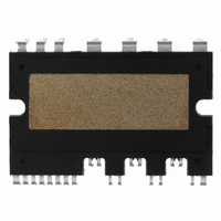
... Fairchild Semiconductor 2.2 Product Line-Up Table 2.1 Lineup of Mini DIP SPM Family Rating Part Number Current (A) FSBB30CH60C 30 FSBB20CH60C 20 FSBB20CH60CT 20 FSBB15CH60C 15 FSBB15CH60CT 15 FSBF15CH60BT 15 FSBF10CH60B 10 FSBF10CH60BT 10 FSBF5CH60B 5 FSBF3CH60B 3 2.3 Applications Motor drive for household electric appliances, such as air conditioners, washing machines, refrigerators, dish washers, and low power industrial applications as well ...
Page 11
... Bottom View Figure 2.2 Pictures and Package Cross section 2008-03-03 V4 Mini DIP SPM Application Note (2008-03-03) 2.65 ( unit : mm ) (a) SPM27-JA 3.1 ( unit : mm ) (b) SPM27-CC, SPM27-EC FAIRCHILD SEMICONDUCTOR - Smart Power Module 11 Mold Resin FRD IGBT LVIC, HVIC Copper Ceramic Mold Resin FRD ...
Page 12
... Outline and Pin Description 3.1 Outline Drawings 2008-03-03 V4 Mini DIP SPM Application Note (2008-03-03) Pin Arrangement CC(L) 2 COM (UL (VL (WL FOD (UH CC(UH B(U) FAIRCHILD SEMICONDUCTOR - Smart Power Module S( (VH CC(VH B( S(V) (WH) CC(WH) B(W) S( ...
Page 13
... V4 Mini DIP SPM Application Note (2008-03-03) (a) SPM27-JA FAIRCHILD SEMICONDUCTOR - Smart Power Module 13 ...
Page 14
... V4 Mini DIP SPM Application Note (2008-03-03) Pin Arrangement CC(L) 2 COM (UL (VL (WL FOD (UH CC(UH B(U) FAIRCHILD SEMICONDUCTOR - Smart Power Module S( (VH CC(VH B( S(V) (WH) CC(WH) B(W) S( ...
Page 15
... Figure 3.1 Package Outline Dimensions 2008-03-03 V4 Mini DIP SPM Application Note (2008-03-03) (b) SPM27-CC, SPM27-EC FAIRCHILD SEMICONDUCTOR - Smart Power Module 15 ...
Page 16
... Negative DC-Link Input for V Phase Negative DC-Link Input for W Phase Output for U Phase 25 V Output for V Phase 26 W Output for W Phase 27 P Positive DC-Link Input 2008-03-03 V4 Mini DIP SPM Application Note (2008-03-03) Table 3.1 Pin descriptions Pin Description FAIRCHILD SEMICONDUCTOR - Smart Power Module 16 ...
Page 17
... The wiring of each input should be as short as possible to protect the Mini DIP SPM against noise influences. • To prevent signal oscillations coupling is recommended as illustrated in Fig. 6.1. 2008-03-03 V4 Mini DIP SPM Application Note (2008-03-03 – V B(W) S( (VH) (WH) FAIRCHILD SEMICONDUCTOR - Smart Power Module 17 ...
Page 18
... V4 Mini DIP SPM Application Note (2008-03-03) to eliminate noise. SC pin should be minimized. SC signal line should be pulled up to the 5V O depends on the capacitance value of C FOD - [F]. (18.3 is internal setting value of FOD FOD FAIRCHILD SEMICONDUCTOR - Smart Power Module 18 and the low-side SC according to the FOD ...
Page 19
... Inverter output pins for connecting to the inverter load (e. g. motor). 3.3 Description of dummy pins Figure 3.2 defines the Mini DIP SPM dummy pins. 2008-03-03 V4 Mini DIP SPM Application Note (2008-03-03) Figure. 3.2 Description of dummy pins FAIRCHILD SEMICONDUCTOR - Smart Power Module 19 ...
Page 20
... B(V) VB CC(H) VCC OUT COM (VH S(V) B(U) VB CC(H) VCC OUT COM (UH S(U) OUT(WL) SC C(SC) FOD C(FOD) FO VFO (WL) OUT(VL) IN(WL) (VL) IN(VL) (UL) IN(UL) COM OUT(UL) CC(L) VCC V SL Figure 4.1 Internal circuit FAIRCHILD SEMICONDUCTOR - Smart Power Module 20 P (27) W (26) V (25) U (24) N (23 (22 (21) U ...
Page 21
... Inverter low-side IGBTs: Gate drive circuit, Short-circuit protection with soft shut-down control, Control supply circuit under-voltage protection • Fault signaling (V ): Corresponding fault (low-side IGBTs fault FO (low-side supply) • Input interface: 3.3V, 5V CMOS/LSTTL compatible, Schmitt trigger input, Active high. 2008-03-03 V4 Mini DIP SPM Application Note (2008-03-03) FAIRCHILD SEMICONDUCTOR - Smart Power Module 21 ...
Page 22
... Short-circuit Operation In case of short-circuit turn-off, the 400V V (100V or less, generated by the stray inductance between the Mini DIP SPM and the DC-link capacitor) from V . PN(Surge) Table 5.1 Detail description of absolute maximum ratings (FSBB15CH60C case) Item Symbol Supply Voltage V PN Supply Voltage (surge) ...
Page 23
... Figure 5.2 Short-circuit current turn-off waveforms @ V 2008-03-03 V4 Mini DIP SPM Application Note (2008-03-03) PN(Surge @Tj= @Tj=125 PN(SURGE) PN(SURGE @Tj=125 @Tj= Hard off PN(SURGE Soft off PN(SURGE Soft off C PN FAIRCHILD SEMICONDUCTOR - Smart Power Module limited to under 500V =450V PN ° =400V, T =125 C j ...
Page 24
... Applied between CC V – COM, V – COM CC(H) CC(L) Applied between – COM IN (UH) (VH) (WH – COM (UL) (VL) (WL) Applied between V – COM FO FO +0.3V, 15V supply interface is possible. However FAIRCHILD SEMICONDUCTOR - Smart Power Module 24 SPM , , (UH) (VH (UL) (VL pins Rating Unit ...
Page 25
... For instance 100Ω and C=1nF for the parts shown dotted in Fig. 6.1. 2008-03-03 V4 Mini DIP SPM Application Note (2008-03-03) SPM 1kΩ Level shift Gate driver circuit 5kΩ(Typical) Gate driver 5kΩ(Typical) Condition Min – COM 2.8 (UH) (VH) (VH – COM - (UL) (VL) (WL) FAIRCHILD SEMICONDUCTOR - Smart Power Module 25 ℃ ) Typ. Max. Unit - - V - 0.8 V ...
Page 26
... IN(VL) (3) IN (UL) IN(UL) (2) COM COM OUT(UL) ( VCC nF, then t = 1.8ms (typ.)). Please refer to the FOD FO and C wiring should be as short as possible should be set in the range of 1~2μsec FAIRCHILD SEMICONDUCTOR - Smart Power Module 26 P (27) W (26) V (25) U (24) N (23 (22 (21 recommended between C FOD FOD ...
Page 27
... Also, since the V capability is 1mA (max), it cannot drive an opto-coupler directly. A buffer circuit should be added in the primary side of the opto-coupler. 2008-03-03 V4 Mini DIP SPM Application Note (2008-03-03) FAIRCHILD SEMICONDUCTOR - Smart Power Module 27 SPC15 output current FO ...
Page 28
... V4 Mini DIP SPM Application Note (2008-03-03) Correct position of Snubber Capacitor SPM Nu,Nv,Nw COM Shunt Resistor FAIRCHILD SEMICONDUCTOR - Smart Power Module 28 If the snubber capacitor is Wiring inductance should be less than 10nH. For example, width > 3mm, thickness = 100μm, length < 17mm in copper pattern ...
Page 29
... IGBT will turn OFF while ignoring the input signal. To prevent noise from interrupting this function, built-in 3μsec filter is installed in both HVIC and LVIC. 2008-03-03 V4 Mini DIP SPM Application Note (2008-03-03) and V ) falls down under UVLO (Under Voltage Lock Out) level FAIRCHILD SEMICONDUCTOR - Smart Power Module 29 ...
Page 30
... Under voltage detection ( UVCCD IGBT OFF in spite of control input condition a5 : Fault output operation starts a6 : Under voltage reset ( UVCCR Normal operation : IGBT ON and carrying current 2008-03-03 V4 Mini DIP SPM Application Note (2008-03-03) Mini DIP SPM Function Operations FAIRCHILD SEMICONDUCTOR - Smart Power Module 30 and the CE(sat) ...
Page 31
... Under voltage detection (UVBSD IGBT OFF in spite of control input condition, but there is no fault output signal Under voltage reset (UVBSR Normal operation: IGBT ON and carrying current 2008-03-03 V4 Mini DIP SPM Application Note (2008-03-03) RESET SET RESET CCR a1 UV CCD FAIRCHILD SEMICONDUCTOR - Smart Power Module ...
Page 32
... Input “L” : IGBT OFF state Input “H”: IGBT ON state, but during the active period of fault output the IGBT doesn’t turn ON IGBT OFF state 2008-03-03 V4 Mini DIP SPM Application Note (2008-03-03) RESET SET RESET b1 UV BSD FAIRCHILD SEMICONDUCTOR - Smart Power Module pin and if this SC ...
Page 33
... SC trip voltage in the LVIC. The drive IC then interrupts low-side IGBT gates to stop IGBT operation. The value of current sensing resistor is calculated by the following expression: V where is the SC reference voltage of the LVIC REF ) 2008-03-03 V4 Mini DIP SPM Application Note (2008-03-03 SET RESET Reference Voltage CR circuit time constant delay REF ) R SHUNT I SC FAIRCHILD SEMICONDUCTOR - Smart Power Module 33 ...
Page 34
... SC circuit malfunction. SC Item Min. Typ. Max. 0.45 0.5 0.55 SC(REF) Min. Typ. Max. - 0 TOTAL FAIRCHILD SEMICONDUCTOR - Smart Power Module 34 Mini DIP SPM COM pin voltage to rises to SC ’ SC(REF) Unit V Unit μsec 0.7 μsec 1.3 ...
Page 35
... For the short circuit state, the diode drop voltage has to be considered to set the SC protection reference level. The equation is as illustrated below. 2008-03-03 V4 Mini DIP SPM Application Note (2008-03-03) 15V-Line CSC R CSC - COM TOTAL V = Vcsc + V SEN F FAIRCHILD SEMICONDUCTOR - Smart Power Module 35 Mini DIP SPM I = 500nA Leakage x C time constant delay (t4 ...
Page 36
... Rating Applied between V -COM -0. Sink current at V pin 5 FO Table 7.5 Electric Characteristics Condition Min. Ω Circuit: 4. Pull-up 4.5 FO Ω Circuit: 4. Pull- [mA] FO terminal MCU SPM GND COM Figure 7.7 V terminal wiring FO FAIRCHILD SEMICONDUCTOR - Smart Power Module 36 Unit +0 Typ. Max. Unit - - 0 ...
Page 37
... V4 Mini DIP SPM Application Note (2008-03-03) C), then a fault signal is released. The protection-timing chart is shown ΔTdr (Hysteresis) SET RESET B ( floating supply can be generated. One of them is the BS FAIRCHILD SEMICONDUCTOR - Smart Power Module 37 SET RESET and V , provides the supply S ( voltage drops below a specified BS is pulled down to ...
Page 38
... V × × × ln( δ − − − (min Out ON V IN(L) N (b) Timing chart of initial bootstrap charging × Δ leak C Δ BS. mainly via the following mechanisms : BS FAIRCHILD SEMICONDUCTOR - Smart Power Module charged through the BS ) (8. (8.2) ...
Page 39
... BS 2008-03-03 V4 Mini DIP SPM Application Note (2008-03-03) voltage is pulled down to ground. Therefore, the on-time S Ω Resistance characteristics supply. Similarly, the high voltage reverse leakage current is important if FAIRCHILD SEMICONDUCTOR - Smart Power Module 39 is only BS capacitor can be fully BS ...
Page 40
... BS (min) V (Voltage drop across the low-side IGBT or load)= 0.7V LS 2008-03-03 V4 Mini DIP SPM Application Note (2008-03-03) -I curve of two bootstrap diode F F voltage is pulled down to ground. It discharges when the high-side IGBT FAIRCHILD SEMICONDUCTOR - Smart Power Module 40 supply when CC ...
Page 41
... These Values depend on PWM Control Algorithm 15V-Line 22uF 1000uF Figure 8.3 Recommended Boot Strap Operation Circuit and Parameters 2008-03-03 V4 Mini DIP SPM Application Note (2008-03-03 ln − − − One-Leg Diagram of SPM Vcc 0.1uF COM VS Vcc 1uF IN OUT V COM SL FAIRCHILD SEMICONDUCTOR - Smart Power Module Inverter Output N ...
Page 42
... Where φ is the phase-angle difference between output voltage and current. Using equations (9.1), the conduction loss of one IGBT and diode can be obtained as follows. 2008-03-03 V4 Mini DIP SPM Application Note (2008-03-03 Threshold voltage of diode on-state slope resistance of diode D FAIRCHILD SEMICONDUCTOR - Smart Power Module 42 (9.1) (9.2) ...
Page 43
... D peak ) cos π 2 π φ − φ − + peak peak ( cos ( × joule ] FAIRCHILD SEMICONDUCTOR - Smart Power Module 43 φ θ (9.3) θ φ θ − cos ( ) d (9.4) (9.5) (9. φ − peak cos π con (9.7) (9.8) (9. for the diode and E can be ...
Page 44
... V4 Mini DIP SPM Application Note (2008-03-03) φ θ φ φ − peak ) d π is used in other cases. Figure 9.1 shows a thermal network of heat θ ja FAIRCHILD SEMICONDUCTOR - Smart Power Module 44 (9.10) and j . When the θ Both the θ usually used θ jc can be θ ca ...
Page 45
... Fig. 9.1 should be considered. For pulsed power loss, the thermal capacitance effect delays the rise in junction temperature, and thus permits a heavier loading of the SPM. Figure 9.2 shows the normalized thermal impedance curves of FSBB30CH60C, FSBB15CH60C, FSBF10CH60B and FSBF3CH60B. The 2008-03-03 V4 Mini DIP SPM Application Note (2008-03-03) ...
Page 46
... FSBB30CH60C 4.0 Z th(J-C)_FRD 3.5 3.0 2.5 2.0 1.5 1.0 0.5 0.0 10 100 1E-6 1E-5 1E-4 (b) FSBB15CH60C 7 Z th(J-C)_FRD 100 1E-6 1E-5 1E-4 1E-3 Pulse Duration [sec] (c) FSBF10CH60B FAIRCHILD SEMICONDUCTOR - Smart Power Module 46 1E-3 0.01 0.1 ...
Page 47
... V4 Mini DIP SPM Application Note (2008-03-03 th(J-C)_FRD 100 1E-6 1E-5 1E-4 1E-3 Pulse Duration [sec] (d) FSBF3CH60B , T ( and P should be measured. Since Voltage Measure Sense Current Device Stirred Dielectic Bath Heater FAIRCHILD SEMICONDUCTOR - Smart Power Module 47 0.01 0 100 , T and P can The Electrical Test Method j ...
Page 48
... DUT. The continuous power heats up the DUT to a thermally equilibrated state. While the device is heating, a continuous train of sampling pulses monitors the TSP, i.e., the voltage drop or the same as the junction 2008-03-03 V4 Mini DIP SPM Application Note (2008-03-03 =m ∗ (V) are used to quantify this straight line o FAIRCHILD SEMICONDUCTOR - Smart Power Module 48 (9.14 ". In this case, V (V) is the f ...
Page 49
... Thermal grease is applied between the SPM and heat sink to prevent an air gap. 2008-03-03 V4 Mini DIP SPM Application Note (2008-03-03) increase of about 100 ℃ above the reference j sensing pulses with 100us is given typically 100us FAIRCHILD SEMICONDUCTOR - Smart Power Module 49 Time measurement of a SPM-IGBT jc and applied c ...
Page 50
... A thermocouple is inserted through the heat sink and pressed against the underside of the SPM to 2008-03-03 V4 Mini DIP SPM Application Note (2008-03-03) Sensing Circuit Device Sense Current m (Tj-Tc θ Air Pressure ON / OFF Switch Thermo -couple Air Blowing FAIRCHILD SEMICONDUCTOR - Smart Power Module Air Pressure Gauge Air Pressure Controller 7mm 125mm ...
Page 51
... Rth(j-c) = Max., M.I.=1.0, P.F=0.8, 3-phase continuous PWM modulation, 60Hz sine waveform output. 100 10 FSBB30CH60C FSBB20CH60C FSBB15CH60C FSBF15CH60BT FSBF10CH60B Figure 9.8 Effective current Note: The above characteristics may vary in the different control schemes and motor drive types. Figure 9.8 indicates an example of an inverter operated under the condition of Tc=125 ° indicates the effective current Io which can be outputted when the junction temperature Tj rises to the average junction temperature of 150 ° ...
Page 52
... This causes an increase in the thermal resistance when the fins are spaced below and above 4mm and 5mm, respectively. An increase in fin thickness decreases the total number of fins and the size of the heat sink, resulting in an increase in thermal resistance. 2008-03-03 V4 Mini DIP SPM Application Note (2008-03-03 FAIRCHILD SEMICONDUCTOR - Smart Power Module θ ha ...
Page 53
... Fin to Fin Spacing, b(mm) Fin to Fin Spacing, b(mm) variation by change of the fin spacing. θ 110 110 130 130 Fin & Base plate length (mm) Fin & Base plate length (mm) variation by change of the base-plate length. θ ha FAIRCHILD SEMICONDUCTOR - Smart Power Module 150 150 170 170 ...
Page 54
... V4 Mini DIP SPM Application Note (2008-03-03 110 110 130 130 150 150 Base plate width, f(mm) Base plate width, f(mm) variation by change of the base-plate width. θ Fin height, c (mm) Fin height, c (mm) variation by change of the fin height. θ ha FAIRCHILD SEMICONDUCTOR - Smart Power Module 54 170 170 ...
Page 55
... A fan having a velocity of 5 m/sec., reduces the resistance to 85% ( ≅ 0.25 ° C/W). Figure 9.15 R 2008-03-03 V4 Mini DIP SPM Application Note (2008-03-03 θ ha variation by change of airflow velocity. θ ha FAIRCHILD SEMICONDUCTOR - Smart Power Module 55 . Two kinds of heat sink base-plates ...
Page 56
... Mounting Torque Mounting Screw : M3 DBC Flatness Heatsink Flatness Weight 2008-03-03 V4 Mini DIP SPM Application Note (2008-03-03) Table 10.1 Torque Rating Condition Recommended 0.62 N⋅m (Note Fig. 10.1) FAIRCHILD SEMICONDUCTOR - Smart Power Module 56 Limits Unit Min. Typ Max 0.51 0.62 1.00 N⋅m μm ...
Page 57
... Do not store devices in the presence of harmful (especially corrosive) gases dusty conditions. 5) Use storage areas where there is minimal temperature fluctuation. Rapid temperature changes can cause moisture condensation on stored devices, resulting in lead oxidation or corrosion result, 2008-03-03 V4 Mini DIP SPM Application Note (2008-03-03 ° FAIRCHILD SEMICONDUCTOR - Smart Power Module 57 ° with humidity kept ...
Page 58
... Ensure that articles (such as clip boards) that are brought into static electricity control areas are constructed of antistatic materials as far as possible. 14) In cases where the human body comes into direct contact with a device, be sure to wear finger cots or gloves protected against static electricity. 2008-03-03 V4 Mini DIP SPM Application Note (2008-03-03) FAIRCHILD SEMICONDUCTOR - Smart Power Module 58 ...
Page 59
... Marking Specifications Figure 10.3 Marking dimension of FSBB15CH60C 2008-03-03 V4 Mini DIP SPM Application Note (2008-03-03) Figure 10.2 Marking layout (bottom side) B ...
Page 60
... F : FAIRCHILD LOGO 2. XXX : Last 3 digits of Lot No. 3. YWW : WORK WEEK CODE ("Y" refers to the below alphabet character table) 4. Hole Side Marking - CP : FSBB15CH60C (Product Name) - XXX : Last 3 digits of Lot No. - YWW : WORK WEEK CODE ("Y" refers to the below alphabet character table) Y 2000 2001 ...
Page 61
... Packaging Specifications Figure 10.4 Description of packaging process for SPM27-CC. 2008-03-03 V4 Mini DIP SPM Application Note (2008-03-03) FAIRCHILD SEMICONDUCTOR - Smart Power Module 61 ...
Page 62
... Figure 10.5 Description of packaging process for SPM27-CC. 2008-03-03 V4 Mini DIP SPM Application Note (2008-03-03) FAIRCHILD SEMICONDUCTOR - Smart Power Module 62 ...
Page 63
... Figure 10.6 Description of packaging process for SPM27-JA. 2008-03-03 V4 Mini DIP SPM Application Note (2008-03-03) FAIRCHILD SEMICONDUCTOR - Smart Power Module 63 ...
Page 64
... Fairchild semiconductor and its agents. Regarding transmission or reproduction of this specification, prior written approval of Fairchild semiconductor is required. Please contact Fairchild semiconductor and its agents if you have any questions about this specification. 2008-03-03 V4 Mini DIP SPM Application Note (2008-03-03) ...