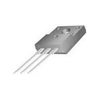
FDPF16N50UT Fairchild Semiconductor, FDPF16N50UT Datasheet - Page 2

FDPF16N50UT
Manufacturer Part Number
FDPF16N50UT
Description
MOSFET N-CH 500V 15A TO-220F-3
Manufacturer
Fairchild Semiconductor
Series
UniFET™r
Datasheet
1.FDPF16N50UT.pdf
(9 pages)
Specifications of FDPF16N50UT
Fet Type
MOSFET N-Channel, Metal Oxide
Fet Feature
Standard
Rds On (max) @ Id, Vgs
480 mOhm @ 7.5A, 10V
Drain To Source Voltage (vdss)
500V
Current - Continuous Drain (id) @ 25° C
15A
Vgs(th) (max) @ Id
5V @ 250µA
Gate Charge (qg) @ Vgs
45nC @ 10V
Input Capacitance (ciss) @ Vds
1945pF @ 25V
Power - Max
38.5W
Mounting Type
Through Hole
Package / Case
TO-220-3 Full Pack, Formed Leads
Transistor Polarity
N-Channel
Resistance Drain-source Rds (on)
0.37 Ohms
Drain-source Breakdown Voltage
500 V
Gate-source Breakdown Voltage
30 V
Continuous Drain Current
15 A
Power Dissipation
38.5 W
Forward Transconductance Gfs (max / Min)
23 S
Gate Charge Qg
32 nC
Mounting Style
Through Hole
Lead Free Status / RoHS Status
Lead free / RoHS Compliant
Available stocks
Company
Part Number
Manufacturer
Quantity
Price
Company:
Part Number:
FDPF16N50UT
Manufacturer:
FSC
Quantity:
245
FDP16N50U / FDPF16N50UT Rev.
Package Marking and Ordering Information
Electrical Characteristics
Off Characteristics
On Characteristics
Dynamic Characteristics
Switching Characteristics
Drain-Source Diode Characteristics
Notes:
1. Repetitive Rating: Pulse width limited by maximum junction temperature
2. L = 5.5mH, I
3. I
4. Pulse Test: Pulse width 300s, Duty Cycle 2%
5. Essentially Independent of Operating Temperature Typical Characteristics
BV
BV
I
I
V
R
g
C
C
C
Q
Q
Q
t
t
t
t
I
I
V
t
Q
DSS
GSS
d(on)
r
d(off)
f
S
SM
rr
T
FS
GS(th)
SD
DS(on)
iss
oss
rss
g(tot)
gs
gd
rr
SD
Device Marking
Symbol
DSS
FDPF16N50UT
J
16A, di/dt 200A/s, V
DSS
FDP16N50U
AS
= 15A, V
Maximum Continuous Drain to Source Diode Forward Current
Maximum Pulsed Drain to Source Diode Forward Current
Drain to Source Diode Forward Voltage
Reverse Recovery Time
Reverse Recovery Charge
Turn-On Delay Time
Turn-On Rise Time
Turn-Off Delay Time
Turn-Off Fall Time
Input Capacitance
Output Capacitance
Reverse Transfer Capacitance
Total Gate Charge at 10V
Gate to Source Gate Charge
Gate to Drain “Miller” Charge
Drain to Source Breakdown Voltage
Breakdown Voltage Temperature
Coefficient
Zero Gate Voltage Drain Current
Gate to Body Leakage Current
Gate Threshold Voltage
Static Drain to Source On Resistance
Forward Transconductance
DD
= 50V, R
DD
BV
FDPF16N50UT
FDP16N50U
G
DSS
= 25, Starting T
Device
Parameter
, Starting T
J
= 25C
J
= 25C
Package
TO-220F
TO-220
I
I
V
V
V
V
V
dI
V
V
V
V
f = 1MHz
V
V
V
R
D
D
DS
DS
GS
DD
GS
GS
GS
GS
DS
DS
DS
GS
G
F
= 250A, V
= 250A, Referenced to 25
/dt = 100A/s
= 25
= 500V, V
= 400V, T
= 0V, I
= ±30V, V
= 40V, I
= 25V, V
= 400V, I
= 250V, I
= 0V, I
= V
= 10V, I
= 10V
DS
T
Test Conditions
, I
C
2
SD
SD
D
Reel Size
D
= 25
D
GS
D
GS
D
= 7.5A
= 15A
= 15A
C
= 7.5A
GS
DS
= 250A
= 15A
= 15A
= 125
= 0V
= 0V, T
o
-
-
= 0V
= 0V
C unless otherwise noted
o
C
J
= 25
(Note 4, 5)
(Note 4, 5)
o
(Note 4)
(Note 4)
o
C
C
Tape Width
-
-
Min.
500
3.0
-
-
-
-
-
-
-
-
-
-
-
-
-
-
-
-
-
-
-
-
-
1495
Typ.
0.37
235
150
0.1
0.5
8.5
65
20
32
14
40
65
80
23
-
-
-
-
-
-
-
-
Quantity
www.fairchildsemi.com
Max.
±100
1945
0.48
310
140
170
250
310
5.0
1.6
90
25
30
45
15
60
50
50
-
-
-
-
-
-
-
Units
V/
nC
nC
nC
pF
pF
pF
C
A
nA
ns
ns
ns
ns
ns
A
A
V
V
V
S
o
C


