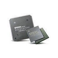
S1D13743F00A200 Epson, S1D13743F00A200 Datasheet - Page 133

S1D13743F00A200
Manufacturer Part Number
S1D13743F00A200
Description
LCD Drivers LCD CNTRL w/Embedded 464KB SRAM
Manufacturer
Epson
Datasheet
1.S1D13743F00A200.pdf
(134 pages)
Specifications of S1D13743F00A200
Maximum Clock Frequency
33 MHz, 68.59 MHz
Operating Supply Voltage
1.5 V
Maximum Operating Temperature
+ 85 C
Package / Case
QFP-20-144
Attached Touch Screen
No
Maximum Supply Current
74 mA
Minimum Operating Temperature
- 40 C
Lead Free Status / RoHS Status
Lead free / RoHS Compliant
Available stocks
Company
Part Number
Manufacturer
Quantity
Price
Company:
Part Number:
S1D13743F00A200
Manufacturer:
EPSON
Quantity:
5 690
- Current page: 133 of 134
- Download datasheet (3Mb)
Epson Research and Development
Vancouver Design Center
X70A-A-001-00
X70A-A-001-00
X70A-A-001-00
Hardware Functional Specification
Issue Date: 2010/05/18
• section 14.1, reworded some of the steps in the Gamma Correction Programming
• section 17, minor wording changes to clarify the Host Interface usage examples
• section 7.1.1 Input Clocks - Table 7-1 Clock Input Requirements (CLKI) - change Input
• section 7.1.2 PLL Clock - change all PLL output min to 44.28 MHz. and all PLL output
• section 7.2.1 Intel 80 Interface Timing - Table 7-3 Intel 80 Input A.C. Characteristics -
• section 8.4 Setting SYSCLK and PCLK - change first equation to “15.03ns < T
• section 2.6 Display Features -change third bullet text paragraph “... must fit inside 232K
• section 7.1.1 Input Clocks - Table 7-1 Clock Input Requirements (CLKI) - change f
• section 7.1.2 PLL Clock - Figure 7-2 PLL Start-Up Time, Table 7-2 PLL Clock
• section 7.2.1 Intel 80 Interface Timing - Table 7-3 Intel 80 Input A.C. Characteristics -
• section 8.4 Setting SYSCLK and PCLK - replace numbers in equations with new,
• section 9 Registers - correct register address typos in introduction
• section 9.1 Register Mapping- correct register address typos
• REG[18h] - add to note “Minimum value of this register = 4 Pixels”
• REG[34h] - add bits 6-3 and change register default to 08h
• REG[54h] - change register default to ??h
• section 17 Host Interface - correct register address typos in introduction note
• section 17.1.5 Individual Memory Location Reads - delete step 1 and re-number steps,
• Engineering changes added
Revision 0.05
Revision 0.04
Revision 0.03
Example
clock frequency - PLL max to 66.53 MHz, and Input clock frequency - CLKI max to
68.59 MHz.
max to 66.53 MHz,
change t
< (T
third equation to “44.28MHz < f
bytes...” to “... must fit inside 228K bytes...”
Max, t3 max, t4 max, t5 min/max, t6 min/max, add note 6
Requirements - change PLL output to min 44.26, max 66.95
change t
replace Figure 8-3 Setting of SYSCLK for a Desired PCLK
changes to note
BBC
odh
odh
- 0.976) ÷ 2.06 ns”, second equation to “15.03ns < T
min to 11.0, and t
and t
ddt
min and max
Revision 2.7
ddt
SYSCLK
min to 2.7 and max to 18.0
< 66.53MHz”
SYSCLK
< 22.584ns”, and
X70A-A-001-02
S1D13743
SYSCLK
Page 133
OSC
Related parts for S1D13743F00A200
Image
Part Number
Description
Manufacturer
Datasheet
Request
R

Part Number:
Description:
Display Modules & Development Tools S1D13743 Eval board
Manufacturer:
Epson

Part Number:
Description:
INK CARTRIDGE, T0803, EPSON, MAG
Manufacturer:
Epson
Datasheet:

Part Number:
Description:
INK CARTRIDGE, T0804, EPSON, YEL
Manufacturer:
Epson
Datasheet:

Part Number:
Description:
CXA1034M
Manufacturer:
EPSON Electronics
Datasheet:

Part Number:
Description:
Manufacturer:
EPSON Electronics
Datasheet:

Part Number:
Description:
Manufacturer:
EPSON Electronics
Datasheet:

Part Number:
Description:
Manufacturer:
EPSON Electronics
Datasheet:

Part Number:
Description:
Manufacturer:
EPSON Electronics
Datasheet:

Part Number:
Description:
RTC58321Real time clock module(4-bit I/O CONNECTION REAL TIME CLOCK MODULE)
Manufacturer:
EPSON Electronics
Datasheet:

Part Number:
Description:
SCI7661DC-DC Converter
Manufacturer:
EPSON Electronics
Datasheet:

Part Number:
Description:
Manufacturer:
EPSON Electronics
Datasheet:

Part Number:
Description:
Manufacturer:
EPSON Electronics
Datasheet:


