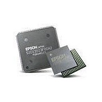
S1D13743F00A200 Epson, S1D13743F00A200 Datasheet - Page 69

S1D13743F00A200
Manufacturer Part Number
S1D13743F00A200
Description
LCD Drivers LCD CNTRL w/Embedded 464KB SRAM
Manufacturer
Epson
Datasheet
1.S1D13743F00A200.pdf
(134 pages)
Specifications of S1D13743F00A200
Maximum Clock Frequency
33 MHz, 68.59 MHz
Operating Supply Voltage
1.5 V
Maximum Operating Temperature
+ 85 C
Package / Case
QFP-20-144
Attached Touch Screen
No
Maximum Supply Current
74 mA
Minimum Operating Temperature
- 40 C
Lead Free Status / RoHS Status
Lead free / RoHS Compliant
Available stocks
Company
Part Number
Manufacturer
Quantity
Price
Company:
Part Number:
S1D13743F00A200
Manufacturer:
EPSON
Quantity:
5 690
- Current page: 69 of 134
- Download datasheet (3Mb)
10.3.9 Miscellaneous Registers
bit 7
bit 1
bit 0
bit 7
REG[56h] Power Save Register
Default = 00h
REG[58h] Non-Display Period Control / Status Register
Default = 00h
PWRSVE Input
Display Period
Vertical Non-
Pin Function
Status (RO)
Epson Research and Development
Vancouver Design Center
Hardware Functional Specification
Issue Date: 2010/05/18
7
7
Horizontal Non-
Display Period
Status (RO)
6
6
PWRSVE Input Pin Function
This bit determines the functionality of the PWRSVE input pin.
When this bit = 0, the PWRSVE pin is OR’d with the Sleep Mode Enable/Disable bit
(REG[56h] bit 1) and setting either to 1 will enable Sleep Mode.
When this bit = 1, the PWRSVE pin is OR’d with the Standby Mode Enable/Disable bit
(REG[56h] bit 0) and setting either to 1 will enable Standby Mode.
Sleep Mode Enable/Disable
This bit controls the Sleep power save mode. Sleep mode can also be controlled by the
PWRSVE pin when REG[56h] bit 7 = 0b.
When this bit = 0, Sleep Mode is disabled (normal operation).
When this bit = 1, Sleep Mode is enabled.
When Sleep Mode is enabled, all internal blocks including the PLL are disabled.
When Sleep Mode is disabled, the PLL requires approximately 10ms lock time before any
memory access should be attempted. The PLL Lock bit, REG[04h] bit 7, can be read to
verify when the PLL becomes stable.
Standby Mode Enable/Disable
This bit controls the Standby power save mode. Standby mode can also be controlled by
the PWRSVE pin when REG[56h] bit 7 = 1b.
When this bit = 0, Standby Mode is disabled (normal operation).
When this bit = 1, Standby Mode is enabled.
When Standby Mode is enabled, all internal blocks are disabled except for the PLL.
When Standby Mode is disabled, the chip can be accessed immediately.
Vertical Non-Display Period Status (Read Only)
This bit indicates whether the LCD panel output is in a vertical non-display period
(VNDP). VNDP is defined as the time between the last pixel on the last line of one frame
to the first pixel on the first line of the next frame.
When this bit = 0, the LCD panel output is in a Vertical Display Period.
When this bit = 1, the LCD panel output is in a Vertical Non-Display Period.
VDP OR’d with
HDP Status
(RO)
5
5
YYC Last Line
n/a
4
4
Revision 2.7
3
n/a
3
TE Output Pin
Enable
2
2
Enable/Disable
TE Output Pin Function Select bits 1-0
Sleep Mode
1
1
Read/Write
Read/Write
Enable/Disable
Standby Mode
X70A-A-001-02
0
0
S1D13743
Page 69
Related parts for S1D13743F00A200
Image
Part Number
Description
Manufacturer
Datasheet
Request
R

Part Number:
Description:
Display Modules & Development Tools S1D13743 Eval board
Manufacturer:
Epson

Part Number:
Description:
INK CARTRIDGE, T0803, EPSON, MAG
Manufacturer:
Epson
Datasheet:

Part Number:
Description:
INK CARTRIDGE, T0804, EPSON, YEL
Manufacturer:
Epson
Datasheet:

Part Number:
Description:
CXA1034M
Manufacturer:
EPSON Electronics
Datasheet:

Part Number:
Description:
Manufacturer:
EPSON Electronics
Datasheet:

Part Number:
Description:
Manufacturer:
EPSON Electronics
Datasheet:

Part Number:
Description:
Manufacturer:
EPSON Electronics
Datasheet:

Part Number:
Description:
Manufacturer:
EPSON Electronics
Datasheet:

Part Number:
Description:
RTC58321Real time clock module(4-bit I/O CONNECTION REAL TIME CLOCK MODULE)
Manufacturer:
EPSON Electronics
Datasheet:

Part Number:
Description:
SCI7661DC-DC Converter
Manufacturer:
EPSON Electronics
Datasheet:

Part Number:
Description:
Manufacturer:
EPSON Electronics
Datasheet:

Part Number:
Description:
Manufacturer:
EPSON Electronics
Datasheet:


