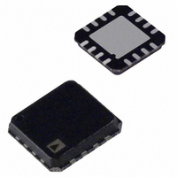
ADXL180WCPZ-RL Analog Devices Inc, ADXL180WCPZ-RL Datasheet - Page 45

ADXL180WCPZ-RL
Manufacturer Part Number
ADXL180WCPZ-RL
Description
IC ACCELEROMETER CONFIG 16-LFCSP
Manufacturer
Analog Devices Inc
Series
iMEMS®r
Datasheet
1.ADXL180WCPZ-RL.pdf
(60 pages)
Specifications of ADXL180WCPZ-RL
Axis
X or Y
Acceleration Range
±50g, 100g, 150g, 200g, 250g, 350g, 500g
Voltage - Supply
5 V ~ 14.5 V
Output Type
Analog
Bandwidth
100Hz ~ 800Hz Selectable
Mounting Type
Surface Mount
Package / Case
16-LFQFN, CSP Exposed Pad
Package Type
LFCSP EP
Operating Supply Voltage (min)
5V
Operating Temperature (min)
-40C
Operating Temperature (max)
125C
Operating Temperature Classification
Automotive
Product Depth (mm)
5mm
Product Height (mm)
1.43mm
Product Length (mm)
5mm
Mounting
Surface Mount
Pin Count
16
Lead Free Status / RoHS Status
Lead free / RoHS Compliant
Sensitivity
-
Interface
-
Lead Free Status / Rohs Status
Compliant
Other names
ADXL180WCPZ-RLCT
TEST AND DIAGNOSTIC TOOLS
V
The V
signal chain from the input of the sensor interface circuitry
(sensor amplifier) through to the output of the current mode
serial port. The function of this pin becomes active after the pin
input voltage exceeds the level of about 0.8 V. Below this level,
the ADXL180 does not respond to the voltage applied to the
V
the V
with the sensor signal.
The applied signal is zero when the input signal is equal to the
common-mode potential of the sensor interface circuitry
(~V
is typically about 640 μV/g. The scaling of the V
to the ADC code output is dependent on the range setting of
the part.
SCI
SCI
DD
pin. Above the threshold limit of 0.8 V, the voltage signal at
SIGNAL CHAIN INPUT TEST PIN
SCI
+600g
–600g
/2 V), see Figure 34. The V
SCI
Figure 34. V
pin is applied to the sensor interface circuitry in parallel
0g
signal chain input test pin allows the excitation of the
SCI
Signal Chain Input Test Pin Transfer Function
~0.8
V
SCI
TEST PIN VOLTAGE
SCI
input scaling for all ranges
V
DD
/2
SCI
~3.2
input voltage
Rev. A | Page 45 of 60
V
The V
the sensor signal chain analog output voltage at the output of
the Bessel filter. This signal is filtered and ranged as defined by
the configuration register settings. It is before the digital auto-
zero function in the signal chain. Therefore, it is not auto-
zeroed. The configuration register SCOE bit must be set to 1 to
enable this output. The signal output resistance is typically
50 Ω. Connect this output to a high impedance input only.
Table 40. SCOE V
SCOE
0
1
Table 41. Typical V
g-Range
50 g
100 g
150 g
200 g
250 g
350 g
500 g
SCO
ANALOG SIGNAL CHAIN OUTPUT TEST PIN
SCO
V
V
conversion is present on V
impedance input, or data or sensor data may be
adversely affected.
Definition
analog signal chain output test pin provides access to
SCO
SCO
output disabled. (Default.)
output enabled. Analog output prior to ADC
SCO
SCO
Signal Chain Output Enable
Sensitivity Per g-Range
Sensitivity
32.8 mV/g
16.4 mV/g
10.8 mV/g
8.2 mV/g
6.56 mV/g
4.69 mV/g
3.28 mV/g
SCO
pin. Connect V
ADXL180
SCO
to high


